
Reverse self aligned double patterning process for back end of line fabrication of a semiconductor device

a semiconductor device and back end technology, applied in semiconductor devices, semiconductor/solid-state device details, electrical devices, etc., can solve the problems of adding complexity and thus cost to the fabrication of semiconductor devices, and achieve the effect of reducing the width of metal structures and cost and complexity

Inactive Publication Date: 2017-04-20
QUALCOMM INC
View PDF1 Cites 32 Cited by
  • Summary
  • Abstract
  • Description
  • Claims
  • Application Information

AI Technical Summary

Benefits of technology

The reverse SADP process allows for the formation of multiple metal structures with different widths and distances between them without using complex masks or multiple masks. This reduces costs and complexity as compared to traditional methods. Additionally, by removing a particular maintained mandrel and the sidewall structures after forming a second hardmask layer, the process enables the formation of different metal structures with different widths and distances between them.

Problems solved by technology

However, using the complex cut / block mask or the multiple masks adds complexity and thus cost to the fabrication of the semiconductor device.

Method used


Image

  • Reverse self aligned double patterning process for back end of line fabrication of a semiconductor device
  • Reverse self aligned double patterning process for back end of line fabrication of a semiconductor device
  • Reverse self aligned double patterning process for back end of line fabrication of a semiconductor device

Examples


Embodiment Construction

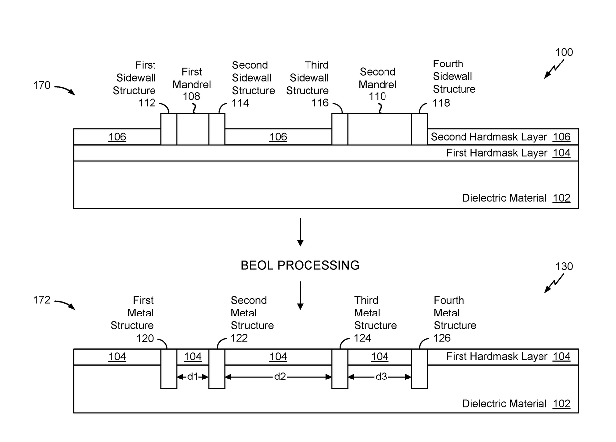
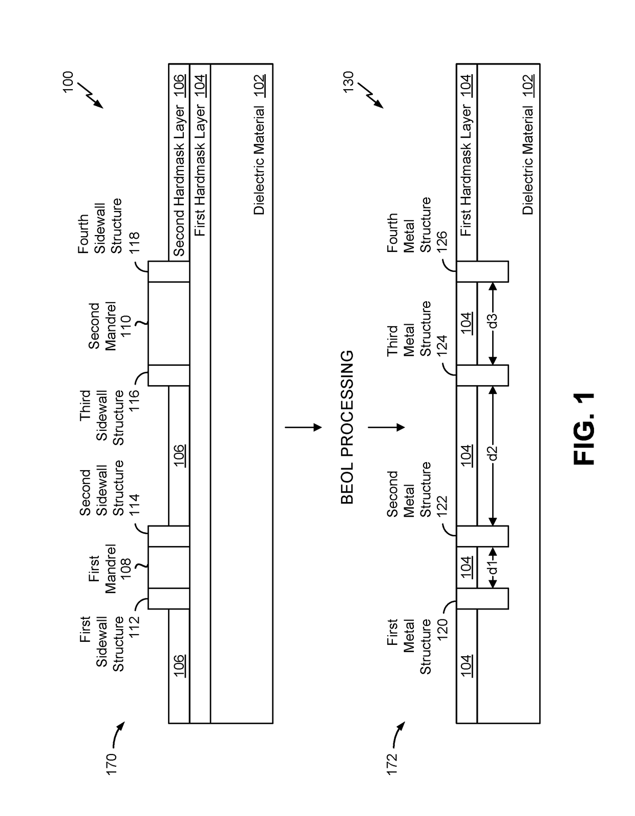
[0031]Referring to FIG. 1, two stages, such as a first stage 100 and a second stage 130, of a first process to fabricate a semiconductor device are depicted. The semiconductor device may include an integrated circuit. A first semiconductor device structure 170 and a second semiconductor device structure 172 may be formed during respective stages of the fabrication process. In a particular embodiment, the second semiconductor device structure 172 represents the semiconductor device formed by the first process. The first process may include a first reverse self aligned double patterning (SADP) process performed during a back-end-of-line (BEOL) fabrication stage of the semiconductor device.

[0032]During the first stage 100, the first semiconductor device structure 170 may include a dielectric material 102, a first hardmask layer 104, a second hardmask layer 106, mandrels 108, 110, and sidewall structures 112-118. The first hardmask layer 104 may be coupled to the dielectric material 102...


PUM


Abstract

In a particular embodiment, a method includes forming a second hardmask layer adjacent to a first sidewall structure and adjacent to a mandrel of a semiconductor device. A top portion of the mandrel is exposed prior to formation of the second hardmask layer. The method further includes removing the first sidewall structure to expose a first portion of a first hardmask layer. The method also includes etching the first portion of the first hardmask layer to expose a second portion of a dielectric material. The method also includes etching the second portion of the dielectric material to form a first trench. The method also includes forming a first metal structure within the first trench.

Description

I. CROSS-REFERENCE TO RELATED APPLICATIONS[0001]The present application claims priority from U.S. patent application Ser. No. 14 / 026,893 filed on Sep. 13, 2013, the contents of which is expressly incorporated by reference in its entirety.II. FIELD[0002]The present disclosure is generally related to forming a semiconductor device using a reverse self aligned double patterning (SADP) process.III. DESCRIPTION OF RELATED ART[0003]Advances in technology have resulted in smaller and more powerful computing devices. For example, there currently exist a variety of portable personal computing devices, including wireless computing devices, such as portable wireless telephones, personal digital assistants (PDAs), and paging devices that are small, lightweight, and easily carried by users. More specifically, portable wireless telephones, such as cellular telephones and internet protocol (IP) telephones, can communicate voice and data packets over wireless networks. Further, many such wireless t...

Claims


Application Information

Patent Timeline
Patent Type & Authority Applications(United States)
IPC IPC(8): H01L21/768H01L21/033H01L23/66H01L23/522H01L23/528
CPCH01L21/76816H01L23/5226H01L23/528H01L23/66H01L2223/6677H01L21/0337H01L21/0338H01L21/76877H01L21/0335H01L21/76838H01L23/485H01L21/31144H01L2924/0002H01L2924/00H01L21/76879G06F30/39
Inventor SONG, STANLEY SEUNGCHULYEAP, CHOH FEIWANG, ZHONGZEZHU, JOHN JIANHONG
Owner QUALCOMM INC
Learn More