Array of encoders for alignment measurement
- Summary
- Abstract
- Description
- Claims
- Application Information
AI Technical Summary
Benefits of technology
Problems solved by technology
Method used
Image
Examples
embodiment 400
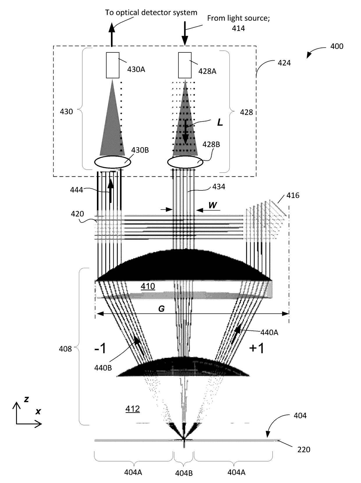
[0047]As shown in the view of FIG. 4, the two first order diffracted beams 440A, 440B respectively correspond to the +1 and −1 orders of diffraction (that is, positive first-order and negative first-order diffraction beams of light), each of which then propagates in a reverse direction through the lens 408. One of the diffracted beams (shown as 440B) is directed through a beamsplitter / beam-combiner 420 towards the output system 430. Another diffracted beam (shown as 440A) is redirected by the reflector 416 to be recombined, spatially overlapped at least in part with the beam 440B at the beamsplitter 420. When recombined at the beamsplitter, the beams 440A, 440B form an output beam 444 that represents a result of optical interference of the beans 440A, 440B and is delivered to the optical detector system 260 of the sensor head through the output system 430. The reflector 416 and the optical beam combiner 420 are preferably equidistantly separated (or distanced or shifted), with respe...
embodiment 900
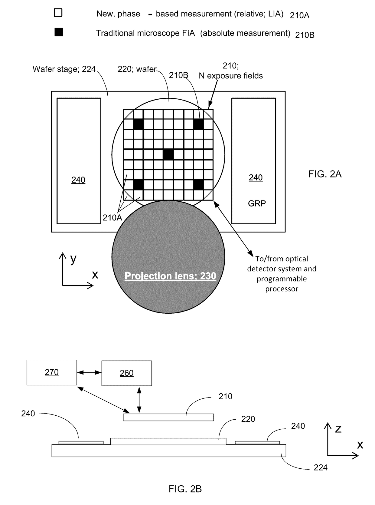
[0068]A specific situation when the operational space above the wafer on the wafer-stage is limited is addressed in a related embodiment, schematically illustrated in FIG. 9. In such a case, the rectangular array 910 of optical heads is configured to contain a total number of optical heads (including the sensor heads 910A and the FIA microscopes 910B) that is smaller than the overall number of exposure fields 140 on the wafer. The specific embodiment 900 of FIG. 9, for example, is configured to contain thirty-two optical heads (three of 910B and twenty-nine of 810A) in the array 910. The measurement of the alignment of all ninety-six exposure fields 140 of the pre-patterned wafer 220 is carried out, in this case, in three steps, during each of which all exposure field within one-third of the wafer that is covered by (located under) the array 910 are measured simultaneously.
[0069]Referring again to FIG. 4, it is also worth noting that, while using a pentaprism as a reflector 416 faci...
embodiment 1100
[0071]In reference to U.S. Pat. No. 6,034,378, the entire disclosure of which is incorporated by reference herein, FIGS. 11A, 11B, 11C present a related embodiment 1100 of the optical measurement sub-system, which includes a pair of compound lenses (or lens systems, comprising multiple lenses) 1110A, 1110B that are coaxially positioned between a reference diffraction grating 1114 of the system and the wafer in-scribe-line diffraction grating structure 1004. The system 1100 also includes (i) an input optic 1118 containing an optical fiber 1118A and a lenslet 1118B disposed to collimate the light output delivered from the facet of the fiber 118A to define a collimated optical beam 1120 in a plane transverse to the common optical axis of the lenses 1110A, 1110B (such as, in one example, the xy-plane as shown); (ii) a fold mirror 1122 (with two reflective surfaces on the opposite sides of the mirror); and (iii) an output optic 1126 containing optical fibers 1126A disposed parallel to th...
PUM
| Property | Measurement | Unit |
|---|---|---|
| width | aaaaa | aaaaa |
| width | aaaaa | aaaaa |
| focal length | aaaaa | aaaaa |
Abstract
Description
Claims
Application Information
 - R&D
- Intellectual Property
- Life Sciences
- Materials
- Tech Scout
- Unparalleled Data Quality
- Higher Quality Content
- 60% Fewer Hallucinations
Browse by: Latest US Patents, China's latest patents, Technical Efficacy Thesaurus, Application Domain, Technology Topic, Popular Technical Reports.
© 2025 PatSnap. All rights reserved.Legal|Privacy policy|Modern Slavery Act Transparency Statement|Sitemap|About US| Contact US: help@patsnap.com


