Method for producing solar cells having simultaneously etched-back doped regions

a technology of solar cells and etching regions, which is applied in the direction of photovoltaic energy generation, sustainable manufacturing/processing, electrical apparatus, etc., can solve the problems of large work and material expenditure in order to etch-back the various, and the doping profiles resulting from the processing may not be optimally configured for their intended use in the solar cell, so as to reduce the amount of work, material and/or time.

Inactive Publication Date: 2017-01-19
UNIV KONSTANZ
View PDF1 Cites 1 Cited by
  • Summary
  • Abstract
  • Description
  • Claims
  • Application Information

AI Technical Summary

Benefits of technology

[0010]There may be a need for a method for producing a solar cell by means of which various doped regions can be formed with a suitable doping profile and in which an outlay in terms of work, material and / or time is reduced as compared with conventional production methods.

Problems solved by technology

The doping profiles resulting from the processing may frequently not be optimally configured for their intended use in the solar cell.
In conventional solar cell production, this results in a considerable outlay in terms of work and material in order to etch-back the various doped regions.

Method used


Image

  • Method for producing solar cells having simultaneously etched-back doped regions
  • Method for producing solar cells having simultaneously etched-back doped regions
  • Method for producing solar cells having simultaneously etched-back doped regions

Examples


Embodiment Construction

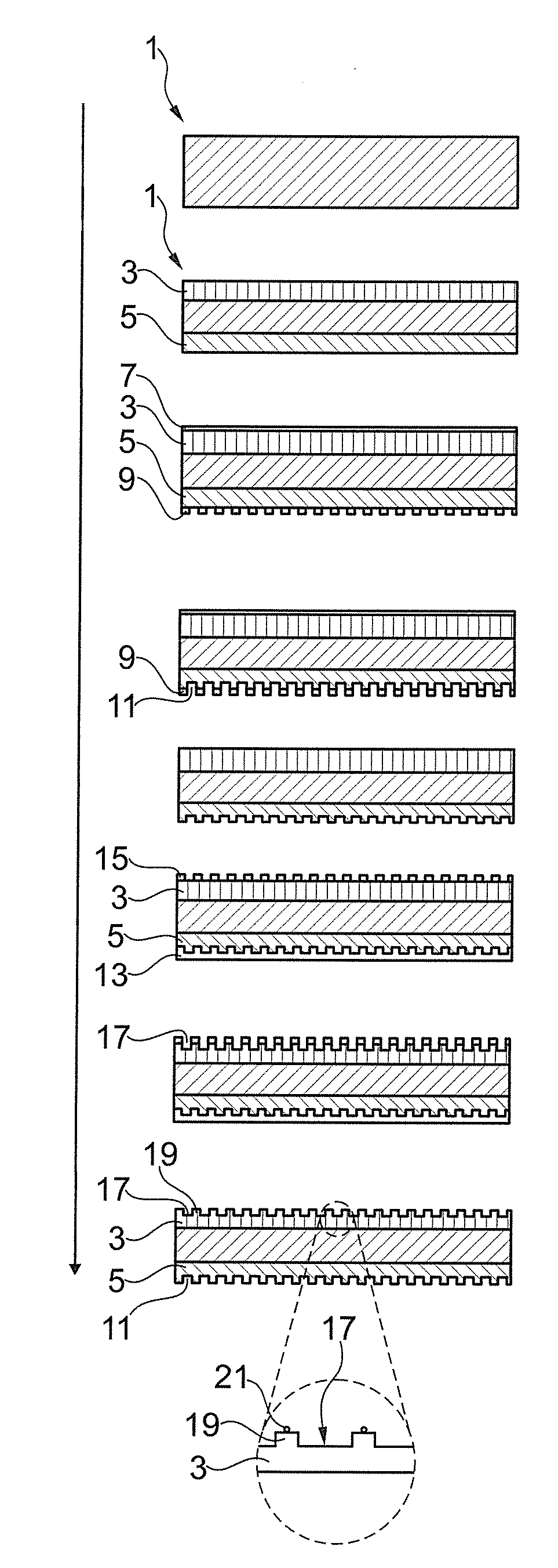
[0053]FIGS. 1 and 2 show sequences of a method for producing a solar cell as have conventionally been used and as are proposed according to embodiments of the present invention, respectively.

[0054]In the case of the conventional production method shown in FIG. 1, a semiconductor substrate 1, for example in the form of a silicon wafer, is first provided (step (a)).

[0055]A plurality of different doped regions 3, 5 are then formed adjacent to a surface of the semiconductor substrate 1. For example, the semiconductor substrate 1 can have a base doping concentration, determined by boron dopants, in the range of from 1015 to 1017 cm−3. In this p-type semiconductor substrate, an n-type emitter-like doped region 3 is produced on the front side by the diffusion of phosphorus. On the back side of the semiconductor substrate 1, a p-type BSF-like doped region 5 is produced by additional diffusion of boron (step (b)).

[0056]Both the emitter-like doped region 3 and the BSF-like doped region 5 are ...


PUM


Abstract

A method for producing a solar cell is described, in which a plurality of doped regions are to be etched-back selectively or over their entire surface. Once a semiconductor substrate (1) has been provided, various doped regions (3, 5) are formed in partial regions of a surface of the semiconductor substrate, the various doped regions (3, 5) differing as regards their doping concentration and/or their doping polarity. The various doped regions (3, 5) are then purposively etched-back in order to achieve desired doping profiles, and finally electrical contacts (21) are formed at least at some of the doped regions (3, 5). The etching-back of the various doped regions takes place in a common etching operation in an etching medium. In order that such common etching-back of various doped regions (3, 5) is possible, it is proposed purposively to adjust both properties of the initially unetched doped regions (3, 5) and parameters that influence the etching operation with regard to properties of the desired doping profiles within the etched doped regions.

Description

FIELD OF THE INVENTION[0001]The present invention relates to a method for producing solar cells having various etched-back doped regions.TECHNOLOGICAL BACKGROUND[0002]Solar cells are used as photovoltaic elements for converting light into electrical energy. To that end, various doped regions are provided in a semiconductor substrate such as, for example, a silicon wafer. The doped regions can differ on the one hand as regards their doping polarity, that is to say they can be n-type doped or p-type doped; on the other hand, the doped regions can also differ as regards the doping concentration, that is to say as regards the density of dopants within the volume of the doped region. On account of different types or densities of charge carriers within the various doped regions, a potential difference is produced at boundaries between adjacent doped regions. By means of such a potential difference, charge carrier pairs which have been generated in the vicinity of those boundaries by absor...

Claims


Application Information

Patent Timeline
Patent Type & Authority Applications(United States)
IPC IPC(8): H01L31/18H01L31/0224
CPCH01L31/022425H01L31/1804H01L31/0684Y02E10/547Y02P70/50
Inventor ENGELHARDT, JOSHFREY, ALEXANDERSCHIELE, YVONETERHEIDEN, BARBARA
Owner UNIV KONSTANZ
Why Eureka
Try Eureka