Optically transmissive antimicrobial glass with shielding effect for electromagnetic wave

a technology of electromagnetic wave shielding and antimicrobial glass, which is applied in the field of antimicrobial glass, can solve the problems of reducing the life of the product, reducing the temperature of the living tissue, and reducing the immune function, so as to achieve long heat treatment time, maintain or even slightly enhance the effect of performan

Active Publication Date: 2016-12-22
THE IND & ACADEMIC COOP IN CHUNGNAM NAT UNIV (IAC)
View PDF2 Cites 0 Cited by
  • Summary
  • Abstract
  • Description
  • Claims
  • Application Information

AI Technical Summary

Benefits of technology

The present invention provides an optically transmissive antimicrobial glass that has an electromagnetic shielding effect. The glass includes an AZO / Ag / AZO multilayer thin film made of about three layers of different compositions deposited on a glass substrate. The AZO single-layer thin film also has antimicrobial properties, but its processing temperature needs to be above 250°C to achieve the same low specific resistance as the multilayer thin film. The thickness of the AZO thin film needs to be at least 250 nm to achieve a specific resistance of -109 Ω·cm or less. The optical transmittance of the thin film gradually decreases with increasing thickness, but it still allows good electromagnetic shielding even at very small thicknesses. The antimicrobial glass has high durability and can be used in electronic equipment that uses a glass panel, particularly touchscreen display panels. It also has an anti-fingerprint characteristic without needing a separate protection film. Overall, the present invention provides a thin, lightweight, and durable solution for protecting electronic equipment from damage caused by external contamination and fingerprints.

Problems solved by technology

Glass is in widespread use for interior / exterior constructive materials largely due to its transparent and aesthetic characteristics but likely to break and vulnerable to fire.
Further, the electromagnetic radiation produced from the circuits mounted in all kinds of electronic equipment possibly causes malfunction of the equipment or electromagnetic interference, eventually with deterioration in the performance of the product and reduction of the product's life span.
Furthermore, the heating effect of the electromagnetic radiation absorbed by the living cells of a human body can raise the temperature of the living tissue to weaken the immune function.
Using the touch screen with one or more fingers leaves fingerprints and smudges on the screen due to dirt and grease of the fingers, which has an adverse effect to spoil the aesthetic of the touch screen.
Further, the touch screen can suffer from the problem of fingerprints on the display that the fingerprint oil residue can deteriorate the clarity of the fingerprints and results in poor definition of the display.
The screen protector is easy to replace but poor in durability and inconvenient to use in that it is likely to be installed on the face of the equipment with air bubbles or imperfect alignment.
This takes a long processing time and lowers the productivity, causing a rise of the production cost.
The heat treatment may be performed at 80 to 150° C. As the extremely low temperature for the heat treatment results in an insufficient surface modification, the desirable temperature for the heat treatment is at least 80° C. But, the angle of contact rather decreases with an increase in the heat treatment temperature, and a high heat treatment temperature is undesirable even in the aspect of the efficiency of the process.

Method used


Image

  • Optically transmissive antimicrobial glass with shielding effect for electromagnetic wave
  • Optically transmissive antimicrobial glass with shielding effect for electromagnetic wave
  • Optically transmissive antimicrobial glass with shielding effect for electromagnetic wave

Examples


example 1

Preparation of Glass Substrate with AZO / Ag / AZO Multilayer Thin Film

[0030]A toughened glass substrate (5 cm×10 cm×70 μm, Corning Gorilla) is washed out and removed of foreign substances from the surface using the N2 gas. Then, an AZO thin film is deposited at the room temperature according to the RF sputtering method. In the deposition process, the AZO target (2 inches in diameter) is a ZnO target doped with 2 wt. % of Al and then sintered at 1,500° C. using the ceramic process (purity: 99.99%). The deposition process is carried out by applying the RF power of 100 W to the target, with the working pressure of 0.13 Pa, the deposition rate of about 1 nm / min and the Ar gas of 10 sccm (standard cc / min) used as a sputtering gas. The thickness of the AZO thin film is controlled by the deposition time.

[0031]On the AZO thin film is in-situ deposited an Ag thin film as thick as 9 nm at the room temperature according to the DC sputtering method. In the deposition process, the target is an Ag t...

example 2

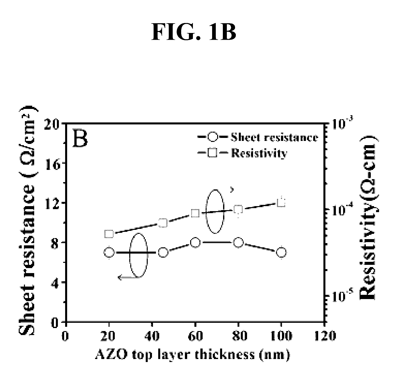
Comparison of Optical / Electrical Characteristics of AZO / Ag / AZO Multilayer Thin Film Depending on Thickness of AZO Thin Film

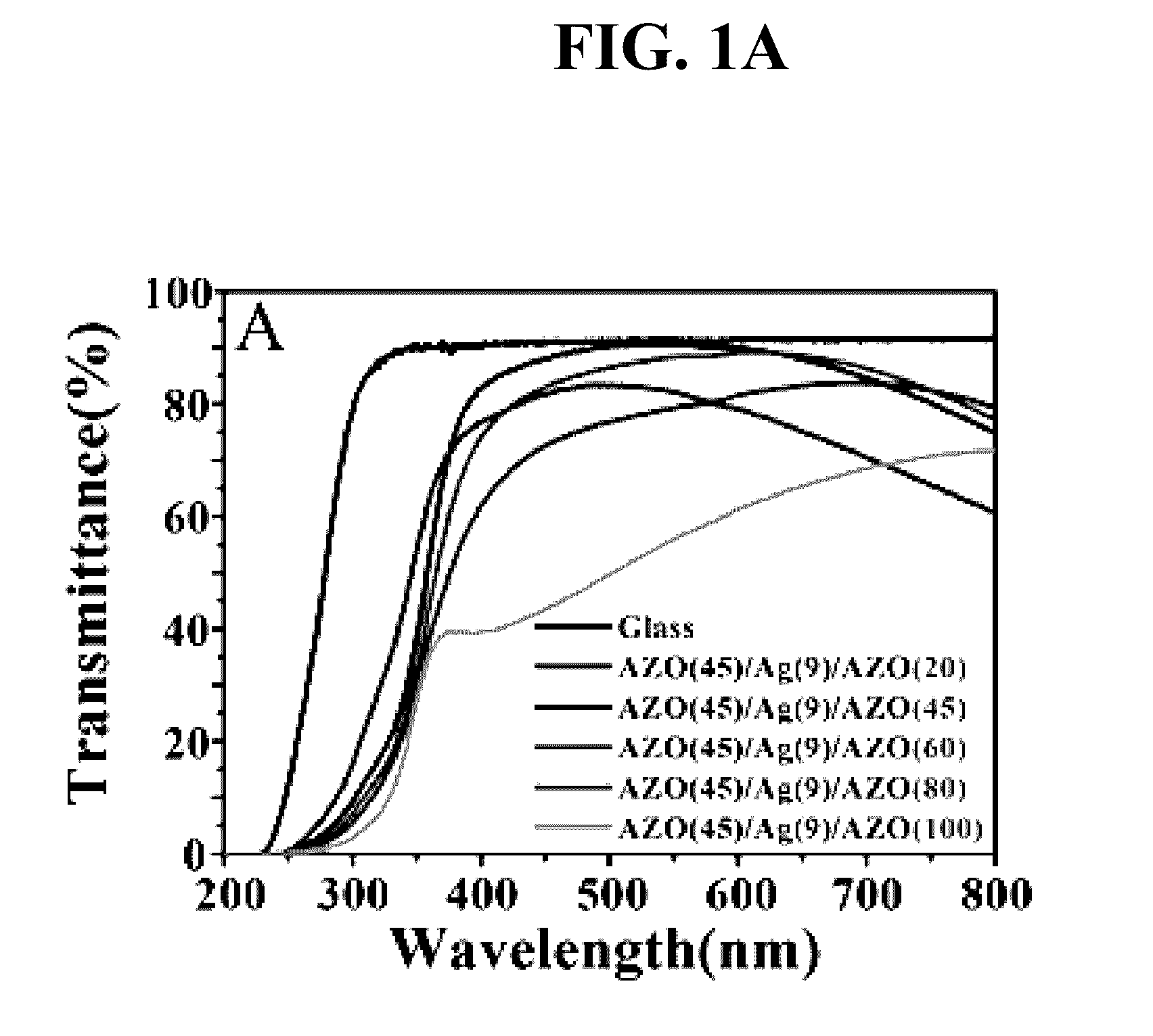
[0033]The glass substrate with the multilayer thin film as prepared in Example 1 is measured in regards to the optical transmittance with an HP 8453 UV-VIS spectrophotometer. The measurement results are presented in FIG. 1A.

[0034]In a pretest for the AZO / Ag / AZO multilayer thin film formed on the toughened glass substrate, the Ag layer formed on the AZO thin film has a non-continuous structure when it is less than 9 nm in thickness, and is continuously deposited when it has a thickness of 9 nm or greater. Accordingly, the optical transmittance gradually increases with an increase in the thickness of the Ag layer from 3 nm to 9 nm, but gradually decreases at the thickness of the Ag layer exceeding 9 nm, and abruptly reduces at the thickness of the Ag layer greater than 15 nm. Thus, the thickness of the Ag layer is fixed at 9 nm.

[0035]FIG. 1A is a graph showing the...

example 3

Evaluation of Electromagnetic Shielding Characteristic for Glass Substrate with AZO / Ag / AZO Multilayer Thin Film

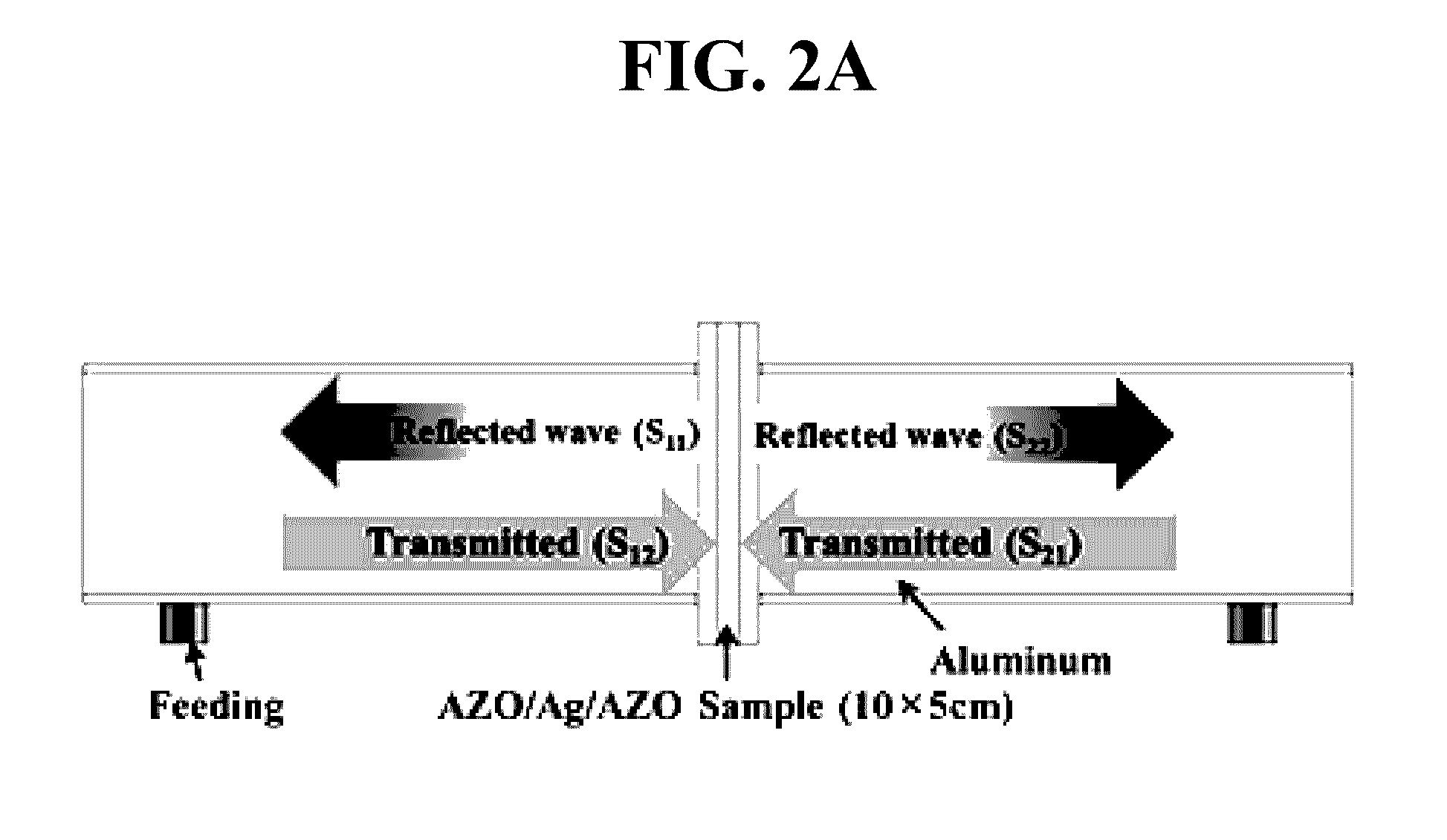
[0037]The glass substrate with the multilayer thin film as prepared in Example 1 is measured in regards to the electromagnetic shielding characteristic in the wavelength range of 1.5 to 3 GHz with an HP Agilent E8363A according to the two-port method. FIG. 2A is a mimetic diagram of an electromagnetic shielding waveguide.

[0038]For a comparison of the electromagnetic shielding characteristic, a Cu film having a thickness of 60 μm is measured in regards to the electromagnetic shielding characteristic under the same conditions. The measurement, S12 value is used to determine the electromagnetic shielding effectiveness according to the following equation. The calculation results are presented in FIGS. 2B, 2C and 3. In FIG. 3, the red dots denote the calculated values of the electromagnetic shielding effectiveness for the Cu film 60 μm thick that is a control.

EMISE=10log1S122=10...


PUM

PropertyMeasurementUnit
thicknessaaaaaaaaaa
thicknessaaaaaaaaaa
contact angleaaaaaaaaaa

Abstract

The present invention relates to an antimicrobial glass having both electromagnetic shielding and antimicrobial characteristics while maintaining the transparency of glass, and more particularly to an optically transmissive antimicrobial glass with an electromagnetic shielding effect that includes an AZO / Ag / AZO multilayer thin film deposited on a glass substrate.

Description

CROSS-REFERENCE TO RELATED APPLICATION[0001]This application claims priority to Korean Application No.: 10-2015-0087578 filed Jun. 19, 2015, which is incorporated herein by reference.TECHNICAL FIELD[0002]The present invention relates to an antimicrobial glass that has both electromagnetic shielding and antimicrobial characteristics while maintaining the transparency of glass.BACKGROUND ART[0003]Glass is in widespread use for interior / exterior constructive materials largely due to its transparent and aesthetic characteristics but likely to break and vulnerable to fire. As toughened glass and fire-resistant glass are available to remedy the disadvantages of glass like breakableness and low resistance to fire, glass has more widespread usages in surface materials for electronic equipment such as mobile phones, home appliances such as refrigerators, air conditioners, etc., tableware, furniture, or the like. With the recent advent of electronic equipment integrated on a glass panel, clea...

Claims


Application Information

Patent Timeline
Patent Type & Authority Applications(United States)
IPC IPC(8): B32B17/06
CPCB32B17/061B32B2307/754B32B2307/412B32B17/06C03C17/36C03C17/3676C03C2217/70C03C17/3644B32B17/1099G02B1/16C03C17/3639C03C17/361G02B1/18C03C23/007
Inventor YOON, SOON-GILCHOI, HUNG-JIN
Owner THE IND & ACADEMIC COOP IN CHUNGNAM NAT UNIV (IAC)
Why Eureka
Try Eureka