Micro-molded electrodes, arrays, and methods of making the same

a micro-electrode and array technology, applied in electroencephalography, diagnostic recording/measuring, applications, etc., can solve the problems of low degree of freedom, and no device identified as the “gold standard"

Active Publication Date: 2016-08-04
UNIV OF UTAH RES FOUND
View PDF18 Cites 13 Cited by
  • Summary
  • Abstract
  • Description
  • Claims
  • Application Information

AI Technical Summary

Benefits of technology

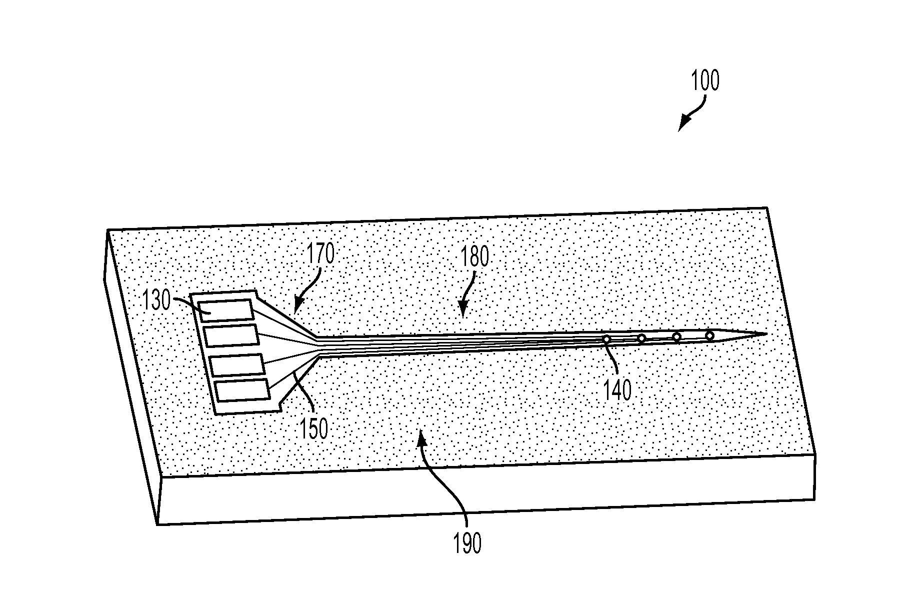
The present technology is about making small electrodes and arrays of them. These electrodes can have customizable dimensions and high aspect ratios. One method involves creating a cavity in a mold and filling it with a conductive material to create a micro-molded electrode. The electrode has multiple sensors along its shaft, each with a bonding pad for electrical connection. The electrode can be coated and combined with other electrodes in 2D or 3D arrays. The invention allows for the creation of small electrodes with customizable dimensions and high aspect ratios.

Problems solved by technology

However, to date, there is no device that has been identified as the “gold standard” in the field.
As a result, the research and technology environment for neural interfaces is still highly limited.
The pursuits of researchers are often limited by technological limitations, inadequate resources, infrastructure and insufficient budget.
Such limitations hamper a researcher's ability to pursue their scientific quest to validate their hypothesis and, hence, delay potential clinical applications.

Method used


Image

  • Micro-molded electrodes, arrays, and methods of making the same
  • Micro-molded electrodes, arrays, and methods of making the same
  • Micro-molded electrodes, arrays, and methods of making the same

Examples


Embodiment Construction

[0024]Before the present invention is disclosed and described, it is to be understood that this invention is not limited to the particular structures, process steps, or materials disclosed herein, but is extended to equivalents thereof as would be recognized by those ordinarily skilled in the relevant arts. It should also be understood that terminology employed herein is used for the purpose of describing particular embodiments only and is not intended to be limiting.

[0025]It must be noted that, as used in this specification and the appended claims, the singular forms “a,”“an,” and “the” include plural referents unless the context clearly dictates otherwise. Thus, for example, reference to “a channel” includes one or more of such particles, reference to “layers” includes reference to one or more of such layers, and reference to “coating” includes one or more of such steps.

Definitions

[0026]In describing and claiming the present invention, the following terminology will be used in acc...


PUM


Abstract

A method of manufacturing a micro-molded electrode (160) having multiple individually addressable sensors (140) along a shaft (180) can include forming a recess in a mold substrate, depositing a structural material therein, depositing a conductive material at specific locations, providing a coating (190), and removing the mold substrate. A micro-molded electrode (160) having a base (170) tapering to at least one shaft (180) can include an electrode substrate, multiple individually addressable sensors (140), and a coating (190).

Description

RELATED APPLICATION[0001]This application claims the benefit of U.S. Provisional Application No. 61 / 877,695, filed Sep. 13, 2013, which is incorporated herein by reference.FIELD OF THE INVENTION[0002]The present invention relates generally to microelectrodes, arrays thereof, and methods of fabrication. Accordingly, the present invention involves the fields of microscale fabrication, materials science, and process control.BACKGROUND[0003]In the last two decades, the field of neuroprosthetics has gained tremendous momentum through the development of novel architectures for neural interfaces. However, to date, there is no device that has been identified as the “gold standard” in the field. As a result, the research and technology environment for neural interfaces is still highly limited. This is due to the constant need and desire to have electrodes and interconnections designed and developed according to unique specifications suited to a particular application, physiological approach,...

Claims


Application Information

Patent Timeline
IPC IPC(8): A61B5/04A61B5/00A61N1/05A61B5/0478
CPCA61B5/685A61B5/04888A61B5/0492A61B5/4029A61N1/0551A61B2562/125A61B5/04001A61B5/0478A61B5/4058A61B5/389A61B5/296A61B5/24A61B5/291
Inventor NEGI, SANDEEPBHANDARI, RAJMOHAN
Owner UNIV OF UTAH RES FOUND
Why Eureka
Try Eureka