Highly Twinned, Oriented Polycrystalline Diamond Film and Method of Manufacture Thereof

a polycrystalline diamond, oriented technology, applied in the field of polycrystalline diamond film, can solve the problems of high cost, limited availability, geometrical dimensions, etc., and achieve the effect of facilitating outstanding surface finishing

Active Publication Date: 2016-05-12
II VI DELAWARE INC
View PDF3 Cites 10 Cited by
  • Summary
  • Abstract
  • Description
  • Claims
  • Application Information

AI Technical Summary

Benefits of technology

The patent text describes the development of a polycrystalline diamond film with improved durability and edge-making ability. The diamond crystallites in the film are oriented in a way that minimizes misalignment, which can cause stress and premature delamination. The film also has a star-shaped crystal morphology that reduces stress and allows for faster growth without compromising the film's mechanical strength. The high level of diamond crystal uniformity allows for excellent surface finishing of the polished diamond surfaces. The polycrystalline diamond film can be used in various applications such as mechanical, optics, detectors, thermal management, electromagnetic wave management, acoustic wave management, wearing, and chemical inertness.

Problems solved by technology

Though diamond is one of the most versatile and most premium materials, its availability is very limited in nature.
Diamond mined from the earth is typically of single crystal with geometrical dimensions that are limited in size, most of the time, too small for industrial uses that require large dimensions.
The diamond crystal that is relatively large in crystal size, relatively pure in chemical contents, and relatively perfect without crystal defects is very expensive, often times, priceless.
Due to such harsh synthetic conditions, reactor sizes are limited, as are the dimensions of the diamond grown from the HTHP process, not to mention its associated high costs in process, equipment, and safety.
In addition, the HTHP process is not able to produce diamond wafers of a large diameter.
It is known in art that CVD growth processes can also successfully grow polycrystalline diamond thin films on different substrates and / or free standing diamond thick films, though very challenging to obtain low stress films or non-cracked diamond of significant size.
Nevertheless, the growth rate of diamond in CVD process, or any other diamond growth process, is generally slow, e.g., in a range from a growth rate of less than 1 micron / hr to a growth rate of a few microns / hr, though there are reports of being able to grow single crystal at a higher growth rate, but with an increased number of defects.
However, growing large diameter diamond films at high growth rates has challenges.
The faster the diamond film grows, the more undesirable Sp2 carbon atoms are incorporated into the diamond film along with the desirable Sp3 carbon atoms due to a lack of time for hydrogen free radicals to etch away the undesirable Sp2 carbon atoms from the diamond film, which results in an increased stress in the diamond film, and, often times, an undesirable quality of the diamond film.
The faster the diamond grows, at the same time, the more diamond crystallites can be misaligned on the diamond film, which can also result in a higher level of stress in the diamond film.
In addition, the larger the diameter of the substrate on which diamond grows, the more the stress is accumulated in the diamond film, which can result in undesirable premature delamination and shattering of the diamond film.
Therefore, the challenge is to successfully grow diamond film fast and large with desirable features, attributes and properties for various applications.

Method used


Image

  • Highly Twinned, Oriented Polycrystalline Diamond Film and Method of Manufacture Thereof
  • Highly Twinned, Oriented Polycrystalline Diamond Film and Method of Manufacture Thereof
  • Highly Twinned, Oriented Polycrystalline Diamond Film and Method of Manufacture Thereof

Examples


example 1

Successful High Speed Growth of Highly Twinned, [110] Oriented Polycrystalline Diamond Film at Temperatures of 1107° C. and 1117° C. for 188 Hours with 3% Methane

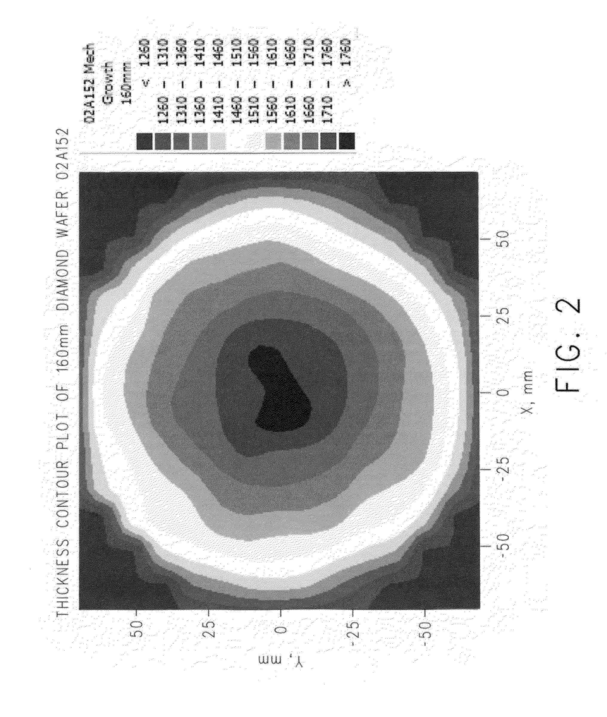
[0135]A piece of metallic tungsten of 160 mm in diameter was used as the substrate 24 in microwave plasma CVD reactor system 2 (FIG. 1). A gas mixture 6 of 2500 mL / min hydrogen and 75 mL / min methane was flowed into the microwave plasma CVD reactor 16. After plasma 20 ignition, the microwave power and the reactor pressure were tuned so that the plasma size covered the entire surface of the metallic tungsten substrate 24. After one hour and 12 minutes of chemical vapor deposition of diamond, hydrogen flow was reduced to 2400 mL / min and methane flow was reduced to 72 mL / min. The diamond growth temperature at the center of the substrate was controlled by cooling substrate 24, e.g., via a thermal-electric cooler in contact with substrate 24 or by a fluid cooling substrate 24. A control pyrometer 26 was used to monitor the temper...

example 5

Successful Growth of Highly Twinned, [110]-Oriented Polycrystalline Diamond Film at 1120° C. in a Separate CVD Reactor for 162 Hours with 3% Methane

[0180]A piece of metallic tungsten of 160 mm in diameter was used as a substrate 24 in a separate microwave plasma CVD reactor 16 similar to the one used in Example 1. A mixture of 2400 mL / min hydrogen and 72 mL / min methane was flowed into the microwave plasma CVD reactor 16 with a methane concentration of 3%, also the same as Example 1. After plasma ignition, the microwave power and the reactor pressure were tuned so that the plasma 20 size covered the entire surface of the metallic tungsten substrate 24. The diamond growth temperature at the center of substrate 24 was controlled at 1120° C. by cooling substrate 24, e.g., via a thermal-electric cooler in contact with substrate 24 or by a fluid cooling substrate 24. A control pyrometer 26 was used to monitor the temperature of the diamond 4 growing at the center of the substrate 24 durin...

example 6

Successful Growth of Highly Twinned, [110]-Oriented Polycrystalline Diamond Film at 1120° C. in a Separate CVD Reactor for 90 Hours with 3% Methane

[0191]A piece of metallic tungsten 160 mm in diameter was used as a substrate 24 in a separate microwave plasma CVD reactor 16 similar to the one used in Example 1. A mixture of 2400 mL / min hydrogen and 72 mL / min methane was flowed into the microwave plasma CVD reactor 16 with a methane concentration of 3%, also the same as Example 1. After plasma ignition, the microwave power and the reactor pressure were tuned so that the plasma 20 size covered the entire surface of the metallic tungsten substrate 24. The diamond growth temperature at the center of substrate 24 was controlled at 1120° C. by cooling substrate 24, e.g., via a thermal-electric cooler in contact with substrate 24 or by a fluid cooling substrate 24. A control pyrometer 26 was used to monitor the temperature of the diamond 4 growing at the center of the substrate during diamo...


PUM

PropertyMeasurementUnit
diameteraaaaaaaaaa
thicknessaaaaaaaaaa
thicknessaaaaaaaaaa

Abstract

In a method of chemical vapor deposition (CVD) growth of a polycrystalline diamond film in a CVD reactor, a gas mixture of gaseous hydrogen and a gaseous hydrocarbon is introduced into the CVD reactor. A plasma formed from the gas mixture is maintained above a surface of a conductive substrate disposed in the CVD reactor and causes a polycrystalline diamond film to grow on the surface of the conductive substrate. A temperature T at the center of the polycrystalline diamond film is controlled during growth of the polycrystalline diamond film. The CVD grown polycrystalline diamond film includes diamond crystallites that can have a percentage of orientation along a [110] diamond lattice direction ≧70% of the total number of diamond crystallites forming the polycrystalline diamond film.

Description

CROSS REFERENCE TO RELATED APPLICATION[0001]This application claims the benefit of U.S. Provisional Application No. 62 / 076,215, filed Nov. 6, 2014, which is incorporated herein by reference.BACKGROUND OF THE INVENTION[0002]1. Field of the Invention[0003]The present invention relates to a polycrystalline diamond film comprising diamond crystallites and a method of growth of the polycrystalline diamond film.[0004]2. Description of Related Art[0005]Diamond is the hardest material known, having a Mohs Hardness of 10, which makes diamond most useful for applications of cutting, machining, drilling, milling, etc. Diamond is also the most thermally conductive material known, having a thermal conductivity up to 2000 to 2200 watts per meter per Kelvin, which makes it highly desirable for applications in thermal management under demanding conditions. Diamond also has an extremely low coefficient of friction, which makes it a versatile material for uses as brakes. Diamond is also an excellent ...

Claims


Application Information

Patent Timeline
Patent Type & Authority Applications(United States)
IPC IPC(8): C30B28/14C30B29/60C30B29/04C01B31/06H01B1/04
CPCC30B28/14C01B31/06C30B29/605C30B29/04H01B1/04C01B32/25C23C16/274C23C16/52C01B32/26C23C16/271C23C16/276
Inventor XU, WEN-QINGLIU, CHAOKRAISINGER, CHARLES J.TANNER, CHARLES D.CURRIER, IANSABENS, DAVIDEISSLER, ELGIN E.ANDERSON, THOMAS E.
Owner II VI DELAWARE INC
Why Eureka
Try Eureka