
Monolithic Tandem Chalcopyrite-Perovskite Photovoltaic Device

Inactive Publication Date: 2016-03-24
IBM CORP
View PDF8 Cites 26 Cited by
  • Summary
  • Abstract
  • Description
  • Claims
  • Application Information

AI Technical Summary

Benefits of technology

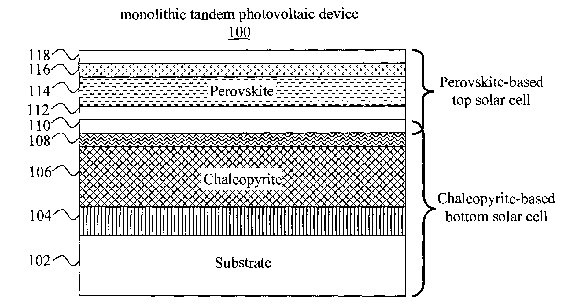
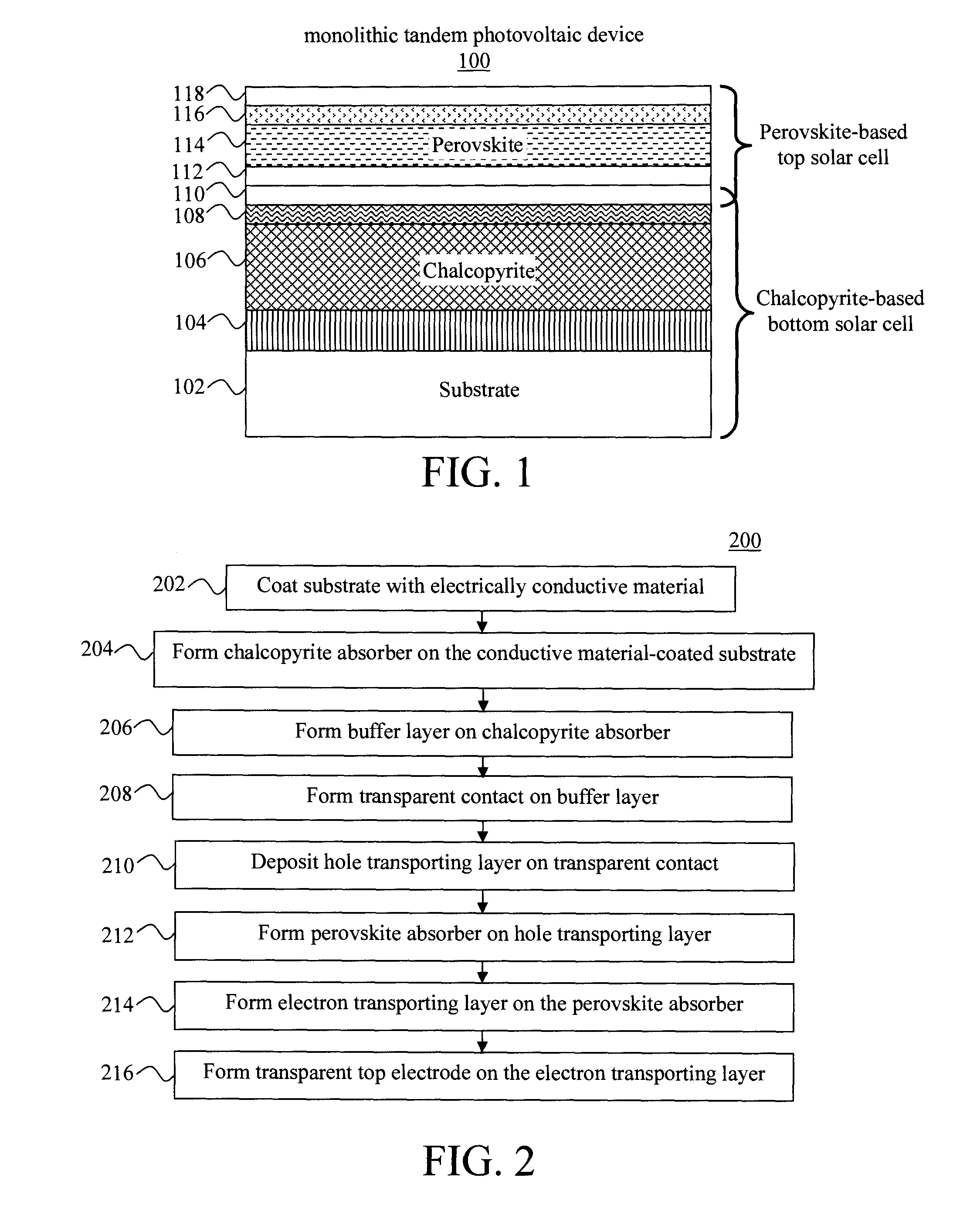
The present invention provides a method for making a monolithic tandem photovoltaic device by which sunlight can be converted into electricity more efficiently using different materials. The device has a layered structure including a substrate, a first solar cell with a layer of chalcopyrite material, a buffer layer, a transparent front contact, a hole transporting layer, a second solar cell with a layer of perovskite material, an electron transporting layer, and a transparent top electrode. The invention is useful for improving the performance of photovoltaic devices.

Problems solved by technology

Two-terminal tandem devices are more challenging to fabricate than four-terminal tandem devices because two-terminal tandem devices require current-matching between the top and bottom solar cells.
While having less strict current-matching and processing constraints than two-terminal devices, four-terminal devices nonetheless suffer from significant resistance and optical losses due to their need for multiple transparent conductive contacts and reflection losses associated with the additional substrates and layers.
The use of chalcogenide-based solar cells in a tandem device architecture however presents some notable challenges.
Thus, chalcogenide-based solar cells often cannot be used as the top solar cell in a tandem device since these high temperatures would degrade the bottom solar cell.
Further, the low band gap of a chalcogenide absorber makes chalcogenide solar cells not well-suited for use in a top cell.
This requirement can be a challenge meet when using conventional solar devices for the top solar cell.

Method used


Image

  • Monolithic Tandem Chalcopyrite-Perovskite Photovoltaic Device
  • Monolithic Tandem Chalcopyrite-Perovskite Photovoltaic Device
  • Monolithic Tandem Chalcopyrite-Perovskite Photovoltaic Device

Examples


Embodiment Construction

[0016]As provided above, due to their high efficiency at a relatively low band gap (about 1.15 electron volts (eV)) chalcogenide-based solar cells are ideal candidates for the bottom solar cells in a tandem device architecture. However, processing temperature constraints limit the options for what top solar cell may be formed on a chalcogenide-based bottom solar cell. Namely, once formed, the chalcogenide-based bottom solar cell should not be subjected to temperatures in excess of about 200 degrees Celsius (° C.).

[0017]Advantageously, the present techniques leverage a new generation of low-cost materials based on methylammonium metal (lead (Pb), tin (Sn)) halide (iodide, chloride, bromide) perovskites which require low processing temperatures (e.g., below 150° C. or even below 80° C.—see below). Perovskite solar cells can have efficiencies exceeding 15%. See, for example, Liu et al., “Efficient planar heterojunction perovskite solar cells by vapour deposition,” Nature vol. 501, 395-...


PUM

PropertyMeasurementUnit
Temperatureaaaaaaaaaa
Electrical conductivityaaaaaaaaaa

Abstract

Monolithic tandem chalcopyrite-perovskite photovoltaic devices and techniques for formation thereof are provided. In one aspect, a tandem photovoltaic device is provided. The tandem photovoltaic device includes a substrate; a bottom solar cell on the substrate, the bottom solar cell having a first absorber layer that includes a chalcopyrite material; and a top solar cell monolithically integrated with the bottom solar cell, the top solar cell having a second absorber layer that includes a perovskite material. A monolithic tandem photovoltaic device and method of formation thereof are also provided.

Description

FIELD OF THE INVENTION[0001]The present invention relates to tandem photovoltaic devices and more particularly, to tandem chalcopyrite (e.g., CIS or CIGS)-perovskite photovoltaic devices and techniques for formation thereof.BACKGROUND OF THE INVENTION[0002]Tandem photovoltaic cells consisting of at least two absorbers with different band gaps allow broader spectrum light harvesting and superior photovoltaic conversion efficiency as compared to single-junction solar cells. Tandem photovoltaic cells are often oriented with one solar cell on top of another. For optimal performance, the bandgap of the absorber in the top solar cell should be higher than the bandgap of the absorber in the bottom solar cell.[0003]Two commonly employed types of tandem device are two-terminal devices and four-terminal devices. Two-terminal tandem devices contain one electrode on top and one electrode on the bottom, with a tunnel junction between the top and bottom solar cells of the device. Four-terminal ta...

Claims


Application Information

Patent Timeline
IPC IPC(8): H01L51/44H01L31/0224H01L31/032H01L31/0687H01L31/18H01L51/42
CPCH01L51/442H01L51/0072H01L31/0687H01L31/022475H01L31/022483H01L31/022491H01L51/4253H01L31/1884H01L2031/0344H01L2251/305H01L2251/308H01L51/004H01L51/0077H01L51/0046H01L2251/10H01L51/0047H01L31/0322Y02E10/549H01L31/06Y02E10/541Y02E10/542Y02E10/544H10K30/57H10K85/1135H10K30/211H10K85/50H10K30/10H10K30/40H10K30/82H01G9/2009H01L31/022441H01L31/0296H01L31/03923H01L31/0725H01L31/0749
Inventor GUHA, SUPRATIKLEE, YUN, SEOGSTURDEVANT, CHARLESTODOROV, TEODOR, K.
Owner IBM CORP
Learn More