Semiconductor device
a technology of semiconductor devices and semiconductors, applied in semiconductor devices, diodes, electrical apparatus, etc., can solve the problems of reducing reliability, affecting the reliability of films b>65/b>, and affecting the reliability of films, so as to prevent the occurrence of cracks, prevent the effect of reducing reliability and preventing an adverse effect on electrical characteristics
- Summary
- Abstract
- Description
- Claims
- Application Information
AI Technical Summary
Benefits of technology
Problems solved by technology
Method used
Image
Examples
embodiment 1
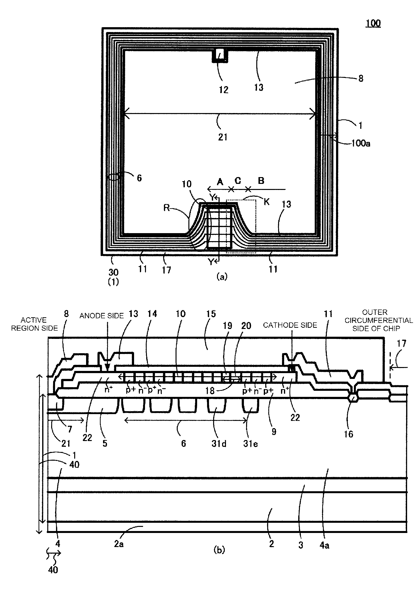
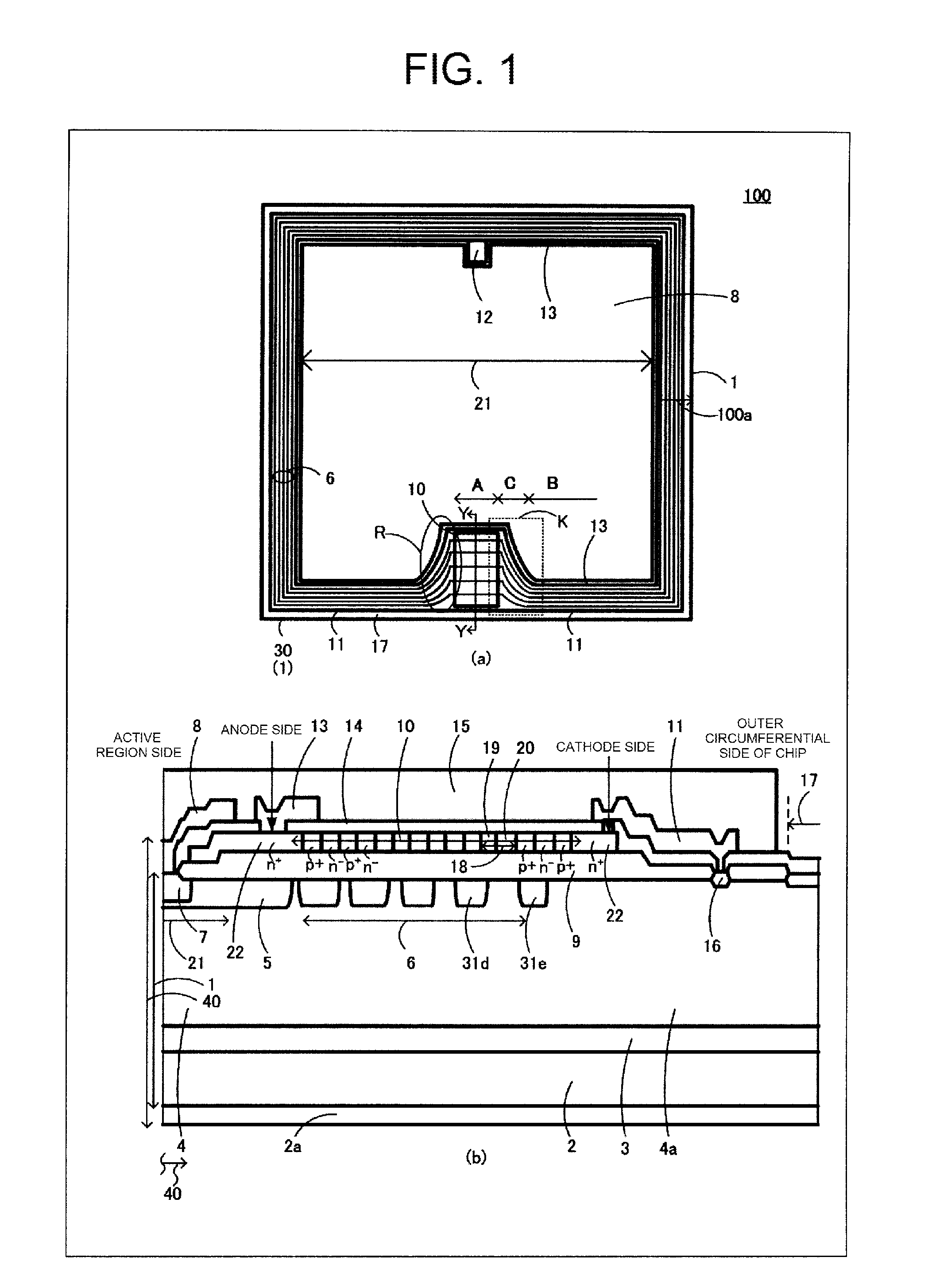
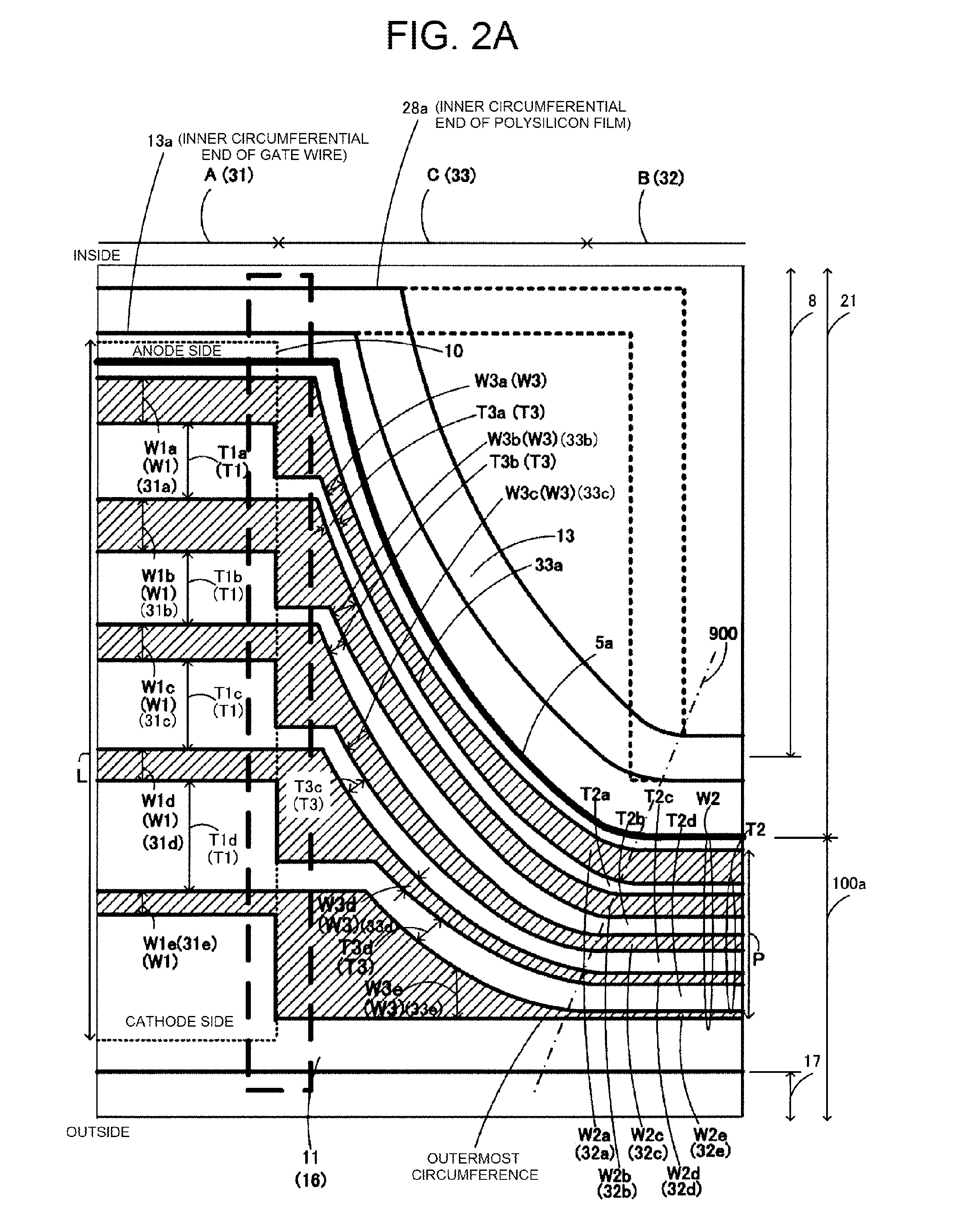
[0056]A semiconductor device 100 according to Embodiment 1 will be described with reference to FIGS. 1 and 9. FIG. 1 is a diagram illustrating the structure of the semiconductor device 100 according to a first example of the invention. FIG. 1(a) is a plan view illustrating a main portion of the semiconductor device 100 according to Embodiment 1. FIG. 1(b) is a cross-sectional view illustrating a main portion of a cross-sectional structure taken along the line Y-Y of FIG. 1(a). The semiconductor device 100 according to Embodiment 1 illustrated in FIG. 1 functions as, for example, an igniter which controls a low-voltage current flowing to a primary coil 505 of an ignition coil of an internal combustion engine ignition device 600 illustrated in FIG. 9.
[0057]Specifically, as illustrated in FIG. 1, the semiconductor device 100 according to Embodiment 1 includes, for example, an IGBT 40 which is a power semiconductor element, a protective diode 10, a gate resistor 502 (not illustrated), a...
example 1
[0090]Next, the protective diode 10 will be described. FIG. 3 is a plan view illustrating the structure of a main portion of the protective diode 10 illustrated in FIG. 1. In the protective diode 10, the p+ layers 19 and the n− layers 20 having a substantially rectangular shape that is elongated in a direction (hereinafter, referred to as a longitudinal direction) perpendicular to the direction in which the p+ layers 19 and the n− layers 20 are alternately arranged are arranged in parallel to the stopper electrode 11 (n-type stopper region 16) that is elongated in the longitudinal direction. Therefore, it is possible to prevent the ends 19a and 20a of the p+ layer 19 and the n− layer 20 in the longitudinal direction from being arranged close to the stopper electrode 11 with a collector potential. As a result, the concentration of the electric field is reduced at the ends 19a and 20a (the ends close to the protective diode 10) of the p+ layer 19 and the n− layer 20 in the longitudina...
example 2
[0096]Next, another example of the semiconductor device according to Embodiment 1 will be described. FIG. 4 is a cross-sectional view illustrating the structure of a main portion of a semiconductor device 200 according to a second example of the invention. FIG. 4 illustrates the vicinity of an outermost guard ring 31e in a first guard ring region 31 and an adjacent guard ring 31d which is provided inside the outermost guard ring 31e. The semiconductor device 200 according to the second example illustrated in FIG. 4 differs from the semiconductor device 100 according to the first example illustrated in FIG. 1 in that one p+ layer 19 (or one n− layer 20) replaces the series pn zener diode 18 which is provided immediately above the space between the outermost guard ring 31e in the first guard ring region 31 and the adjacent guard ring 31d provided inside the outermost guard ring 31e (on the field oxide film 9 which is provided on the surface of a portion of the n− region 4a interposed ...
PUM
 Abstract
Description
Claims
Application Information
 - R&D
- Intellectual Property
- Life Sciences
- Materials
- Tech Scout
- Unparalleled Data Quality
- Higher Quality Content
- 60% Fewer Hallucinations
Browse by: Latest US Patents, China's latest patents, Technical Efficacy Thesaurus, Application Domain, Technology Topic, Popular Technical Reports.
© 2025 PatSnap. All rights reserved.Legal|Privacy policy|Modern Slavery Act Transparency Statement|Sitemap|About US| Contact US: help@patsnap.com


