
Integrated conductive substrate, and electronic device employing same

a technology of integrated conductive substrates and electronic devices, which is applied in the direction of electroluminescent light sources, thermoelectric devices, electric lighting sources, etc., can solve the problems of increasing production costs, reducing the service life of oled devices, and simplifying research for realizing oled devices without additional charge transport layers, etc., to achieve excellent mechanical strength, large-scale manufacturing, and excellent mechanical properties

Inactive Publication Date: 2015-11-12
POSTECH ACAD IND FOUND
View PDF2 Cites 22 Cited by
  • Summary
  • Abstract
  • Description
  • Claims
  • Application Information

AI Technical Summary

Benefits of technology

The patent is for a conductive material that can be used as a substrate and electrode in electronic devices. It has strong mechanical properties, smooth surface, and good conductivity. It is flexible and can be made in large quantities at a low cost. This material can be advantageously used in air-stable electronic devices like OLEDs or OPVs.

Problems solved by technology

However, as several layers are applied, a production cost is increased, and thus in consideration of commercialization, research for realizing an OLED device simplified without an additional charge transport layer is a very important issue.
However, when a conventional oxide electrode such as ITO or FTO, which is disposed on a glass substrate, is bent so as to cause a crack in a thin film, it cannot serve as an electrode any more.
In addition, although the conventional glass substrate is used since a substrate should also withstand a process of depositing a metal oxide performed in a high temperature process at 200° C. or more, the glass substrate is not flexible.

Method used


Image

  • Integrated conductive substrate, and electronic device employing same
  • Integrated conductive substrate, and electronic device employing same
  • Integrated conductive substrate, and electronic device employing same

Examples


example 1

Manufacture of Integrated Conductive Substrate

[0187]A copper foil (thickness: 100 μm) having a first surface having a root mean square roughness (Rq) measured by an atomic force microscope of 30 nm was prepared as a metal layer by preparing a commercially-available copper foil having a surface having a root mean square roughness (Rq) measured by an atomic force microscope of 215 nm, and performing electro-polishing once.

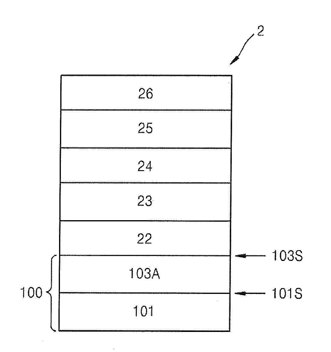
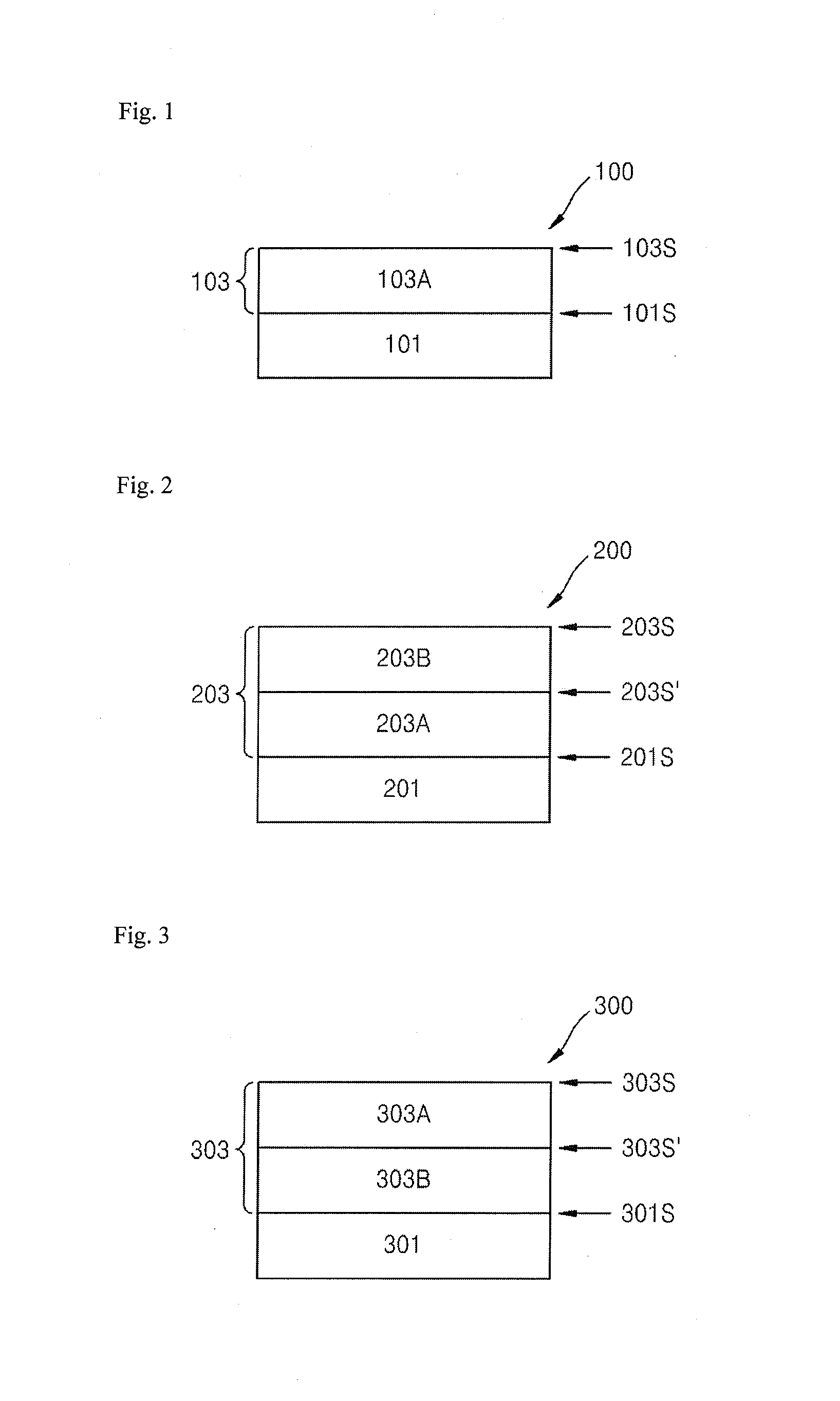
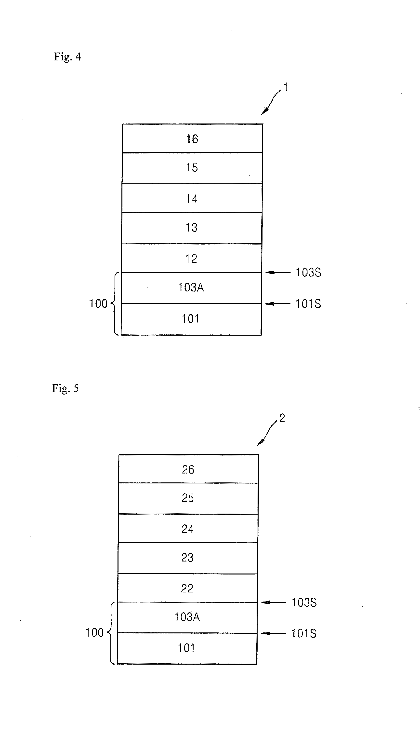
[0188]Subsequently, an integrated conductive substrate was formed of a copper foil metal layer and a ZnO semiconductor layer (formed of a ZnO planarization layer) by preparing a sol-gel first mixture by mixing zinc acetate dehydrate (Sigma Aldrich Inc.) with a mixed solvent of 2-methoxy ethanol and ethanol amine (0.1 g / ml, a volume ratio of 96:4), forming a semiconductor layer with a ZnO planarization layer having a thickness of 40 nm by spin-coating the sol-gel first mixture on a first surface of the copper foil and performing thermal treatment at 400° C. for 30 min...

example 2

Manufacture of Integrated Conductive Substrate

[0197]A copper foil (thickness: 100 μm) having a first surface having a root mean square roughness (Rq) measured by an atomic force microscope of 30 nm was prepared as a metal layer by preparing a commercially-available copper foil having a surface having a root mean square roughness (Rq) measured by the atomic force microscope of 215 nm, and performing electro-polishing once.

[0198]Subsequently, an integrated conductive substrate was formed of a copper foil metal layer and a ZnO semiconductor layer (formed of a ZnO planarization layer and a ZnO intermediate layer) by preparing a sol-gel first mixture by mixing zinc acetate dehydrate (Sigma Aldrich Inc.) with a mixed solvent of 2-methoxy ethanol and ethanol amine (0.1 g / ml, a volume ratio of 96:4), forming a ZnO planarization layer having a thickness of 30 nm by spin-coating the sol-gel first mixture on a first surface of the copper foil and performing thermal treatment at 400° C. for 30 ...

example 3

Manufacture of Integrated Conductive Substrate

[0203]A copper foil (thickness: 100 μm) having a first surface having a root mean square roughness (Rq) measured by an atomic force microscope of 30 nm was prepared as a metal layer by preparing a commercially-available copper foil having a surface having a root mean square roughness (Rq) measured by the atomic force microscope of 215 nm, and performing electro-polishing once.

[0204]Subsequently, an integrated conductive substrate was formed of a copper foil metal layer and a ZnO semiconductor layer (formed of a ZnO intermediate layer and a ZnO planarization layer) by forming a ZnO intermediate layer having a thickness of 20 nm by depositing ZnO on a first surface of the copper foil using a sputter deposition method, and forming a ZnO planarization layer having a thickness of 30 nm by spin-coating a sol-gel first mixture prepared by mixing zinc acetate dehydrate (Sigma Aldrich Inc.) with a mixed solvent of 2-methoxy ethanol and ethanol am...


PUM


Abstract

Provided are an integrated conductive substrate simultaneously serving as a substrate and an electrode, and an electronic device using the same. The integrated conductive substrate includes a metal layer composed of a non-ferrous metal, which has a first surface having a first root mean square roughness, and a semiconductor layer containing a semiconductor material, which has a second surface having a second root mean square roughness and is formed on the first surface. Here, the semiconductor layer includes a semiconductor-type planarization layer formed by a solution process using at least one of the semiconductor material and a precursor of the semiconductor material to planarize the first surface of the metal layer, and the second root mean square roughness is smaller than the first root mean square roughness.

Description

TECHNICAL FIELD[0001]The present invention relates to an integrated conductive substrate and an electronic device using the same.BACKGROUND ART[0002]An organic light emitting diode (OLED) is a self-emissive device having a wide viewing angle, an excellent contrast ratio, a fast response time, a high brightness, a high drive voltage and a high response speed, and capable of multi-colorization.[0003]A general OLED may include a transparent substrate, an anode, a cathode, and an organic layer interposed between the anode and the cathode. The organic layer may include a hole injection layer, a hole transport layer, an emitting layer, an electron transport layer, and an electron injection layer. Holes injected from the anode are transferred to the emitting layer via the hole transport layer, and electrons injected from the cathode are transferred to an emitting layer via the electron transport layer. The carriers such as the holes and the electrons are recombined in the emitting layer re...

Claims


Application Information

Patent Timeline
Patent Type & Authority Applications(United States)
IPC IPC(8): H01L51/00H01L51/52H01L21/02H01L51/44H10K99/00
CPCH01L51/0096H01L51/442H01L21/02425H01L51/5215H01L51/5221Y02E10/549H05B33/26H01L21/02554H01L21/02565H01L21/0262H10K77/10H10K2102/101H10K50/82H10K50/816H10K30/81H10K30/865H10K2102/302H10K30/82H10K50/818
Inventor LEE, TAEWOOKIM, YOUNGHOON
Owner POSTECH ACAD IND FOUND
Learn More