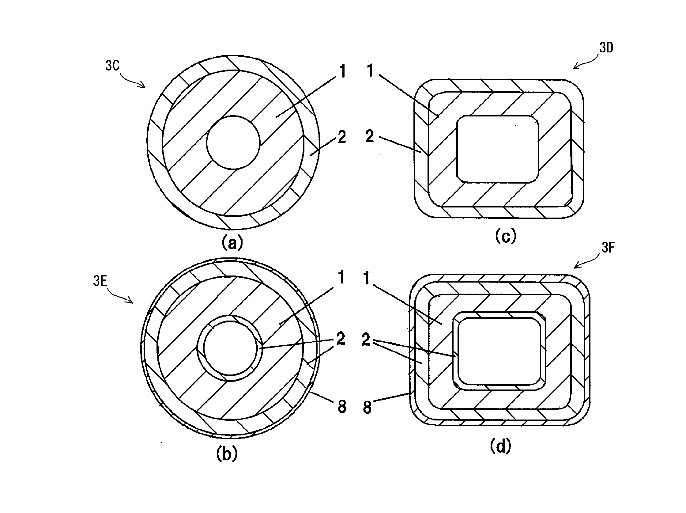
Enamel resin-insulating laminate, insulated wire using the same and electric/electronic equipment
a technology of enamel resin and insulating wires, which is applied in the direction of insulated conductors, cables, conductors, etc., can solve the problems of low voltage decay due to connection cables, high steep voltage rise, and high voltage rise of output pulses due to high-speed switching devices such as igbt, so as to improve the voltage in the inception of partial discharge, improve the effect of dielectric breakdown and thermal aging-resistant properties
- Summary
- Abstract
- Description
- Claims
- Application Information
AI Technical Summary
Benefits of technology
Problems solved by technology
Method used
Image
Examples
example 1
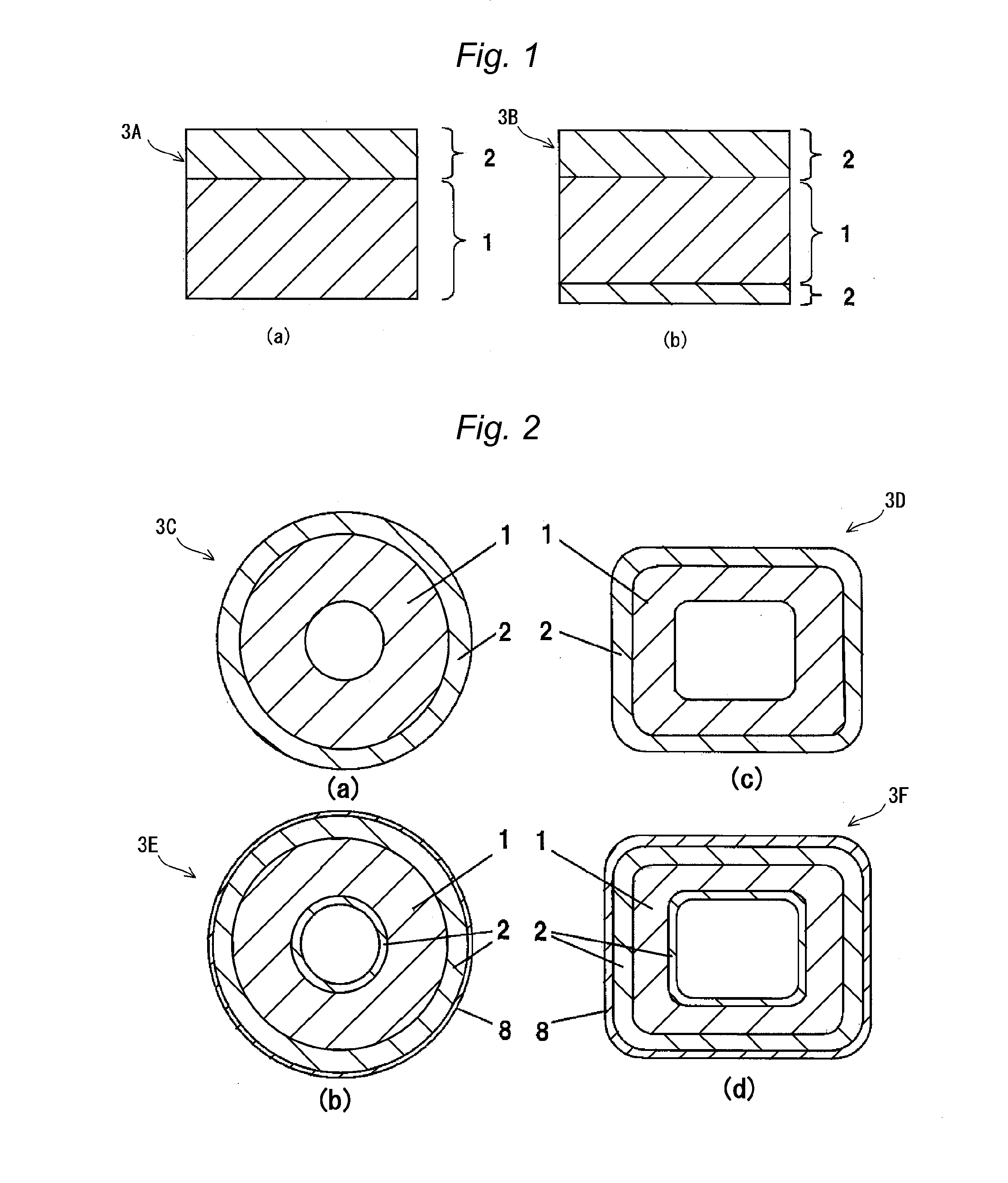
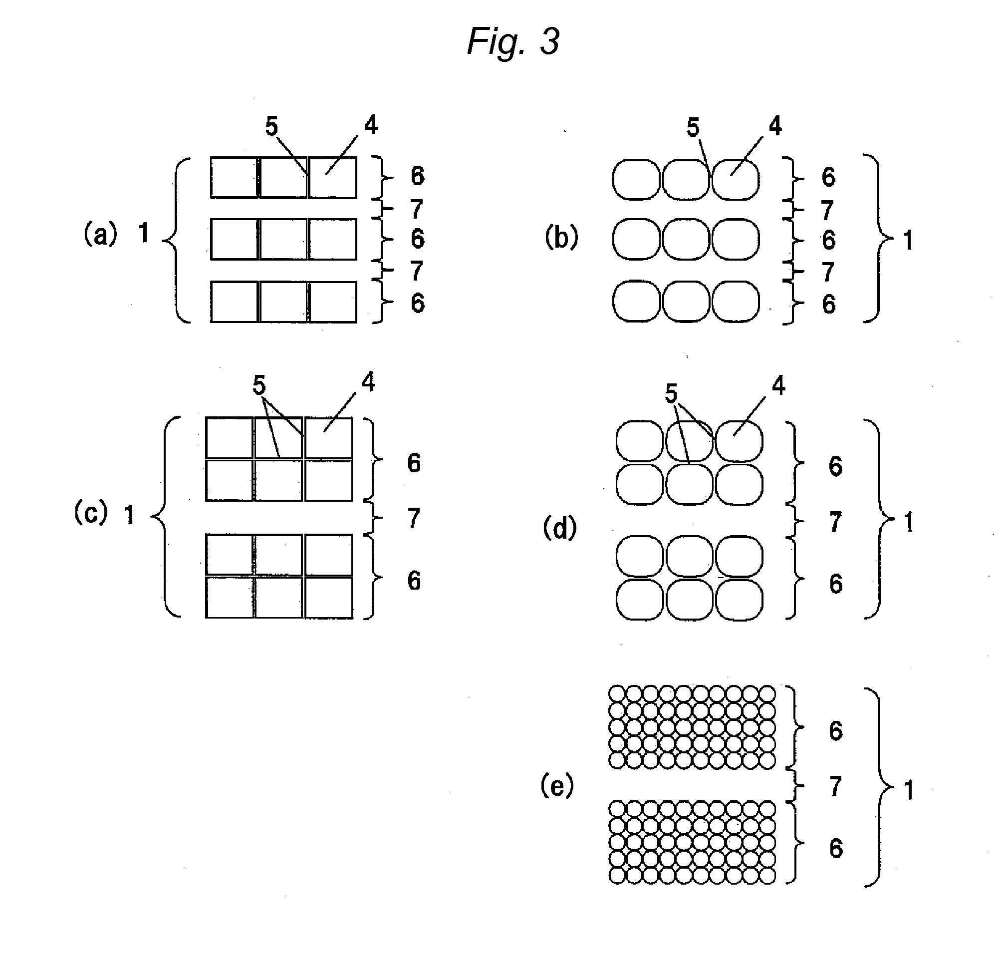
[0137]In Example 1, the insulated wire shown in FIG. 4(a) was produced. The insulated wire had an enamel resin-insulating laminate including foamed region 1 and non-foamed region 2, foamed region 1 having double-layered cell layers 6 and single-layered non-cell layer 7 as shown in FIG. 3(d).
[0138]Specifically, PAI varnish (A) for cell formation was applied onto the periphery of copper wire (conductor) 9 having a diameter of 1 mm, and the resultant material was baked once at a furnace temperature of 520° C. for 20 seconds to form cell layer 6 on the conductor. Onto the periphery of the thus formed cell layer 6, PAI varnish (HI-406 (trade name), a solution containing 33% by mass of resin component, manufactured by Hitachi Chemical Co., Ltd.) was applied, and the resultant material was baked twice for 20 seconds to form non-cell layer 7, and onto the periphery of non-cell layer 7, PAI varnish (A) for cell formation was applied, and the resultant material was baked once for 20 seconds t...
example 2
[0139]The insulated wire shown in FIG. 4(a) was produced in a manner similar to the procedure in Example 1 except that PAI varnish (C) for cell formation was baked at a furnace temperature of 500° C. in place of PAI varnish (A) for cell formation.
example 3
[0140]The insulated wire shown in FIG. 4(a) was produced in a manner similar to the procedure in Example 1 except that an enamel resin-insulating laminate including foamed region 1 and non-foamed region 2 as shown in FIG. 3(b) was formed by baking PAI varnish (A) for cell formation three times and by baking PAI varnish (E) twice in terms of times of baking.
PUM
| Property | Measurement | Unit |
|---|---|---|
| relative dielectric constant | aaaaa | aaaaa |
| thickness | aaaaa | aaaaa |
| thickness | aaaaa | aaaaa |
Abstract
Description
Claims
Application Information
 - R&D
- Intellectual Property
- Life Sciences
- Materials
- Tech Scout
- Unparalleled Data Quality
- Higher Quality Content
- 60% Fewer Hallucinations
Browse by: Latest US Patents, China's latest patents, Technical Efficacy Thesaurus, Application Domain, Technology Topic, Popular Technical Reports.
© 2025 PatSnap. All rights reserved.Legal|Privacy policy|Modern Slavery Act Transparency Statement|Sitemap|About US| Contact US: help@patsnap.com


