It is another object of the present invention is to increase the isolation strength of the base isolation of power semiconductor modules, whereby these modules maybe additionally provided with metal coatings (at ground potential or at another potential) for sensors and / or drive circuits of the substrate, and to improve the partial discharge characteristics.
The present invention relates to a power semiconductor module with high isolation strength that achieves high isolation strength from a base through selectively positioning a plurality of metal coatings on first and second surfaces and positioning edges of the plurality to beneficially reduce the field strength tangentially to a selected position, especially in a defined critical region directly adjacent a metal coating edge on the first surface. This results in providing regions which beneficially allow field lines to extend without functional detriment. The beneficial selection is is achieved by means of an optimization process in which the tangential components of the field strength beside the first or second metallization edge reach identical values.
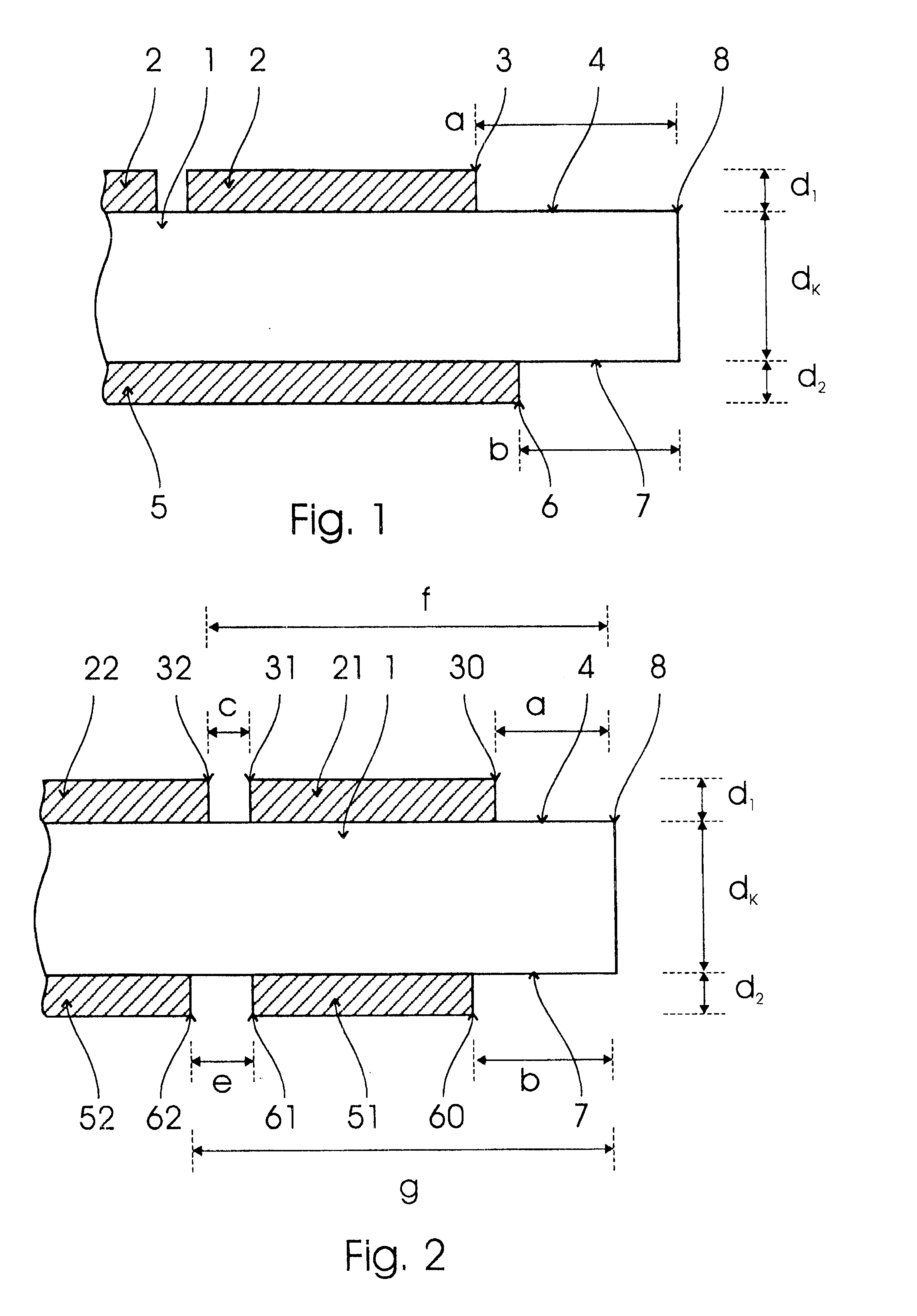
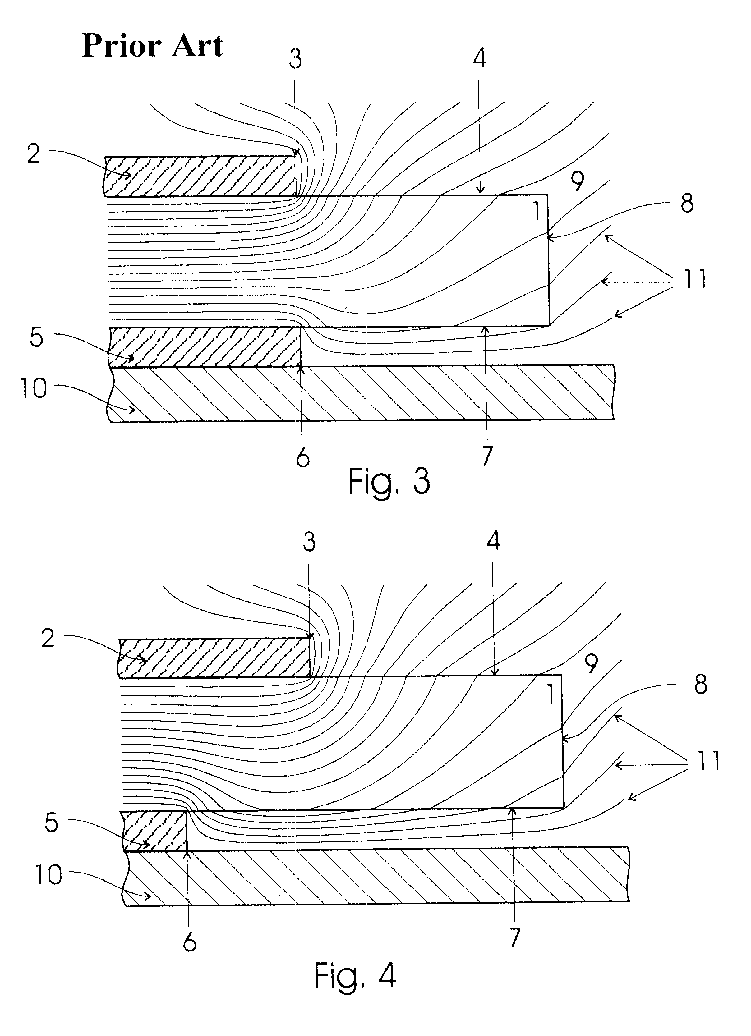
According to an embodiment of the present invention, there is provided a power semiconductor module, including connective elements enabling effective operation and at least one semiconductor component, the power semiconductor module comprising: at least one substrate, the substrate having at least a first surface opposite a second surface, a substrate edge on the substrate joining the first and the second surface, at least a first metal coating on a first surface of the substrate, at least a second metal coating on a second surface of the substrate, the second metal coating between the second surface and a facing surface, the first metal coating having a first metal coating edge, the first metal coating edge a distance a from the substrate edge, the second metal coating having a second metal coating edge, at least the first metal coating edge at a high potential to the substrate edge during an operation of the power semiconductor module, the second metal coating edge a distance b from the substrate edge, and the distance a being less than the distance b, whereby field lines existing between the first metal coating and the second metal coating, and through the substrate, during the operation, beneficially extend away from the second surface opposite the first metal coating edge, thereby beneficially reducing a tangential component of a field strength proximate the first metal coating edge, reducing the field strength and field density on the first surface, and increasing an isolation strength of a base isolation of the substrate.
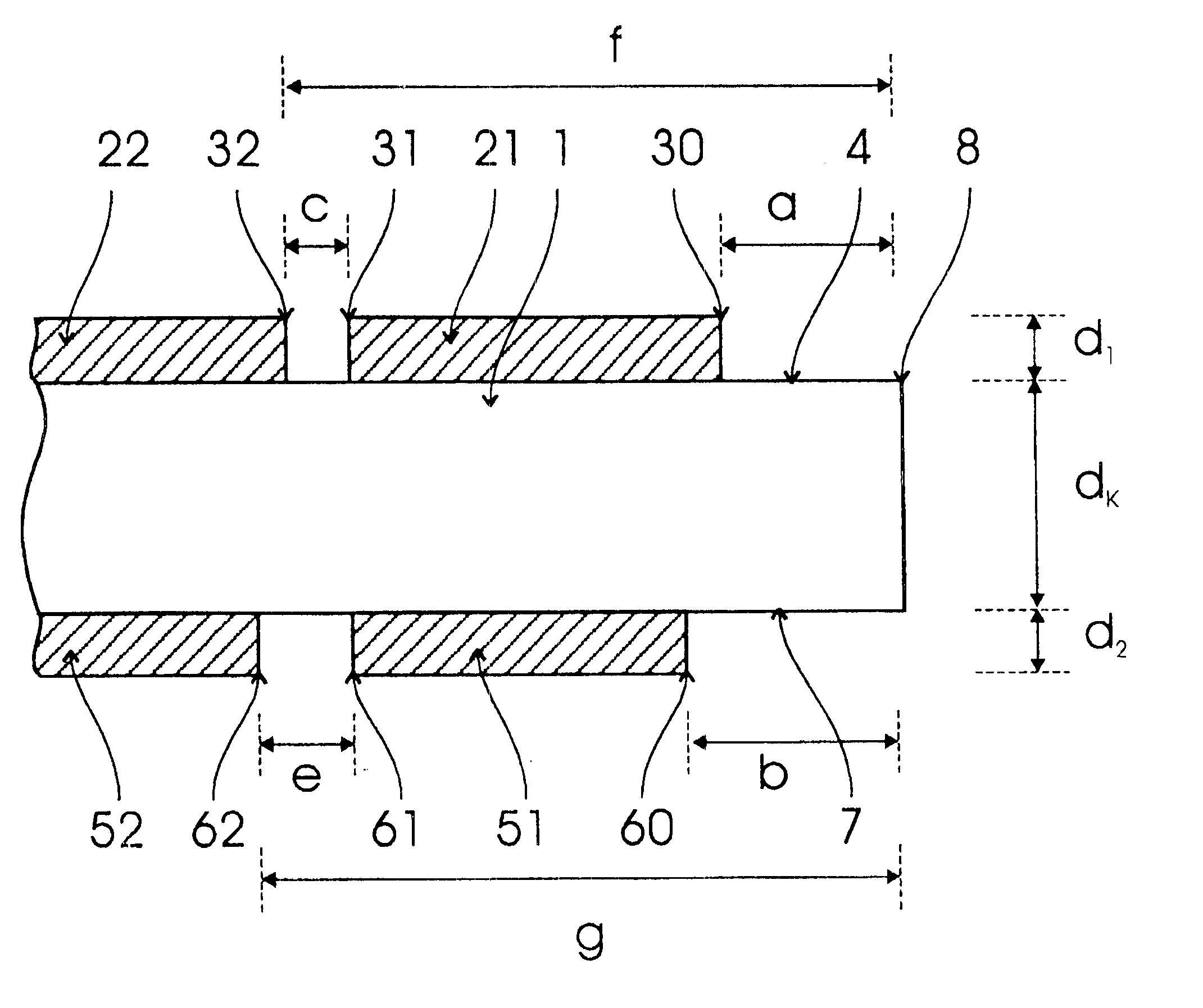
According to another embodiment of the present invention there is provided, a power semiconductor module, including connective elements enabling effective operation and at least one semiconductor component, the power semiconductor module comprising: at least one substrate, the substrate having at least a first surface opposite a second surface, a substrate edge on the substrate joining the first and the second surface, at least a first metal coating on a first surface of the substrate, at least a second metal coating on a second surface of the substrate, the second metal coating between the second surface and a facing surface, the first metal coating having a first metal coating edge, the first metal coating edge a distance f from the substrate edge, the second metal coating having a second metal coating edge, at least the first metal coating edge at a higher potential to the substrate edge during an operation of the power semiconductor module than at least a third metal coating on the first surface between the first metal edge and the substrate edge, the third metal coating having a third metal coating edge opposite the first metal coating edge and a fourth metal coating edge, the second metal coating edge a distance g from the substrate edge, and the distance f being less than the distance g, whereby field lines existing between the first, the second, and the at least third metal coating, and through the substrate, during the operation, beneficially extend away from the second surface opposite the first metal coating edge, thereby beneficially reducing a tangential component of a field strength proximate the first metal coating edge, reducing the field strength and field density on the first surface, and increasing an isolation strength of a base isolation of the substrate.
According to another embodiment of the present invention there is provided a power semiconductor module, further comprising: at least fourth metal coating on the second surface of the substrate between the second metal coating and the substrate edge, the at least fourth metal coating having a fifth metal coating edge opposite the second metal coating edge and a sixth metal coating edge, the third metal coating edge and the fifth metal coating edge at similar distances from the substrate edge, a distance c between the first metal coating edge and the third metal coating edge, a distance e between the second metal coating edge and the fifth metal coating edge, and the distance c being less than the distance e, whereby a density of field lines adjacent the first metal coating edge are widened and the field strength on the first surface of the substrate is beneficially reduced.
According to another embodiment of the present invention there is provided a power semiconductor module, further comprising: at least a fifth metal coating on the first surface between the third metal coating and the substrate edge, at least a sixth metal coating on the second surface between the fourth metal coating and the substrate edge, the fifth metal coating having a seventh metal coating edge adjacent the fourth metal coating edge and an eight metal coating edge, the sixth metal coating having a ninth metal coating edge adjacent the sixth metal coating edge and a tenth metal coating edge, a distance h defined between the fourth metal coating edge and the seventh metal coating edge and equivalent to the distance c, a distance I defined between the sixth metal coating edge and the ninth metal coating edge and equivalent to the distance e, and the eighth metal coating edge being nearer to the substrate edge than the seventh metal coating edge, whereby the distances e, I, f, g, and c are selected to equalize tangential components of the field strength proximate the first and the seventh metal coating edge with tangental components of the field strength proximate the second and the ninth metal coating edge, thereby, reducing the field strength and field density on a non-coated region of the first surface, and increasing an isolation strength of a base isolation of the substrate.


