Piezoelectric element, piezoelectric actuator, piezoelectric sensor, hard disk drive, and inkjet printer device
a piezoelectric actuator and actuator technology, applied in the field of piezoelectric actuators, piezoelectric sensors, hard disk drives, inkjet printer devices, etc., can solve the problems of reducing the reliability of the element, reducing the efficiency of the piezoelectric layer, and unable to achieve the function of an actual piezoelectric element easily, so as to improve the piezoelectric characteristics, and reduce the leakage current
- Summary
- Abstract
- Description
- Claims
- Application Information
AI Technical Summary
Benefits of technology
Problems solved by technology
Method used
Image
Examples
first embodiment
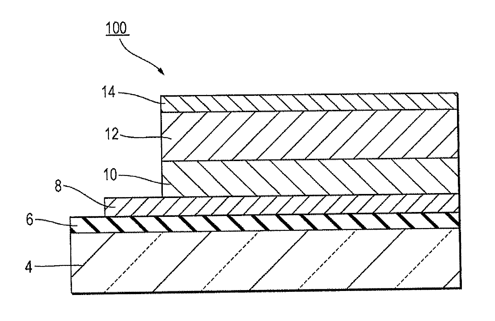
[0039]FIG. 1 shows a piezoelectric element 100 according to the present embodiment. The piezoelectric element 100 includes a substrate 4, an insulating layer 6 and a first electrode layer 8 disposed on the substrate 4, a first piezoelectric layer 10 disposed on the first electrode layer 8, a second piezoelectric layer 12 disposed on the first piezoelectric layer 10, and a second electrode layer 14 disposed on the second piezoelectric layer 12.
[0040]A silicon substrate exhibiting (100) surface orientation can be used as the substrate 4. The substrate 4 has, for example, a thickness of 50 μm or more and 1,000 μm or less. In addition, a silicon substrate exhibiting surface orientation different from a (100) plane, a Silicon on Insulator (SOI) substrate, a quartz glass substrate, a compound semiconductor substrate made from, for example, GaAs, a sapphire substrate, a metal substrate made from, for example, stainless steel, a MgO substrate, a SrTiO3 substrate, or the like can also be use...
second embodiment
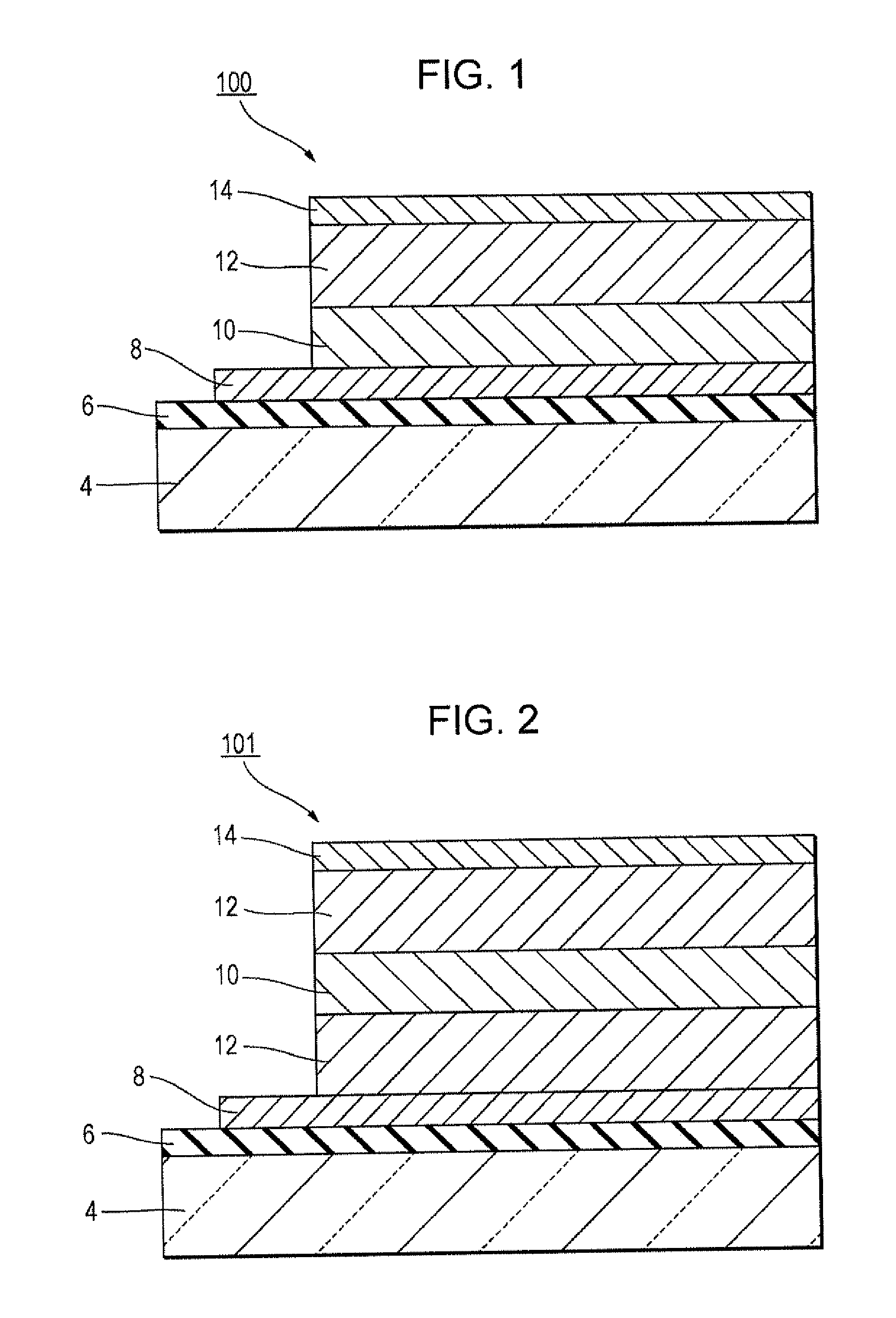
[0059]FIG. 2 shows a piezoelectric element 101 according to the present embodiment. The parts other than the first piezoelectric layer 10 and the second piezoelectric layer 12 are the same as those in the first embodiment. In the piezoelectric element 101, a piezoelectric layer has a configuration in which a first piezoelectric layer 10 is sandwiched between two second piezoelectric layers 12.
[0060]At least two layers of both the second piezoelectric layer 12 and the first piezoelectric layer 10 may be disposed. In that case, a configuration in which the first piezoelectric layer 10 is disposed neither between the second piezoelectric layer 12 and the first electrode layer 8 nor between the second piezoelectric layer 12 and the second electrode layer 14 can be employed. In the case where this configuration is employed, the leakage current of the piezoelectric element 101 can be reduced.
[0061]Up to this point, preferred embodiments of the piezoelectric element according to the presen...
example 1
[0102]In the present example, a term “base member” refers to a member to be provided with a film in each step.
[0103]A silicon wafer (substrate 4) which was provided with a thermal oxidation film (SiO2: insulating layer 6) and which had a diameter of 3 inches was placed in a vacuum chamber of a RF sputtering apparatus, evacuation was performed and, thereafter, a film of Pt was formed as a first electrode layer 8. The base member temperature in film formation was specified to be 400° C. and the thickness of the first electrode layer 8 was specified to be 200 nm.
[0104]Subsequently, the base member was transferred to a chamber of a RF sputtering apparatus equipped with a plurality of sputtering targets, evacuation was performed and, thereafter, a (K0.5Na0.5)NbO3 thin film was formed as a first piezoelectric layer 10. As for a sputtering target, a (K0.5Na0.5)NbO3 sintered material was used. The base member temperature in film formation was specified to be 550° C. and the thickness of the...
PUM
 Abstract
Description
Claims
Application Information
 - R&D
- Intellectual Property
- Life Sciences
- Materials
- Tech Scout
- Unparalleled Data Quality
- Higher Quality Content
- 60% Fewer Hallucinations
Browse by: Latest US Patents, China's latest patents, Technical Efficacy Thesaurus, Application Domain, Technology Topic, Popular Technical Reports.
© 2025 PatSnap. All rights reserved.Legal|Privacy policy|Modern Slavery Act Transparency Statement|Sitemap|About US| Contact US: help@patsnap.com


