Film forming system

a film forming and film technology, applied in the direction of coatings, liquid surface applicators, electrical devices, etc., can solve the problem of requiring a lot of time to perform the film forming treatment on all the chips, and achieve the effect of suppressing the supply amount of coating solution

Inactive Publication Date: 2015-01-15
TOKYO ELECTRON LTD
View PDF3 Cites 3 Cited by
  • Summary
  • Abstract
  • Description
  • Claims
  • Application Information

AI Technical Summary

Benefits of technology

The present invention relates to a method for coating a substrate with a coating film. The grinding of the coating film is performed in a separate grinding apparatus, which avoids the need to supply the coating solution to adjust the film in the coating apparatus. This reduces the amount of coating solution used. After grinding, the substrate is cleaned to prepare for further treatment. The substrate is transferred using two dedicated transfer arms, one for clean substrates and one for dirty substrates, to prevent foreign substances from adhering to another substrate. This method allows for proper treatment of coated substrates with multiple circuits on the front surface while minimizing the amount of coating solution used.

Problems solved by technology

In the case where the coating film is formed on a chip basis as in the prior art under such circumstances, a lot of time is required to perform the film forming treatment on all of the chips because the number of chips is large.
In addition, to adjust the coating film during the spin coating, a large amount of coating solution needs to be supplied onto the wafer because the desired film thickness of the coating film to be formed on the wafer is large.

Method used


Image

  • Film forming system
  • Film forming system
  • Film forming system

Examples


Embodiment Construction

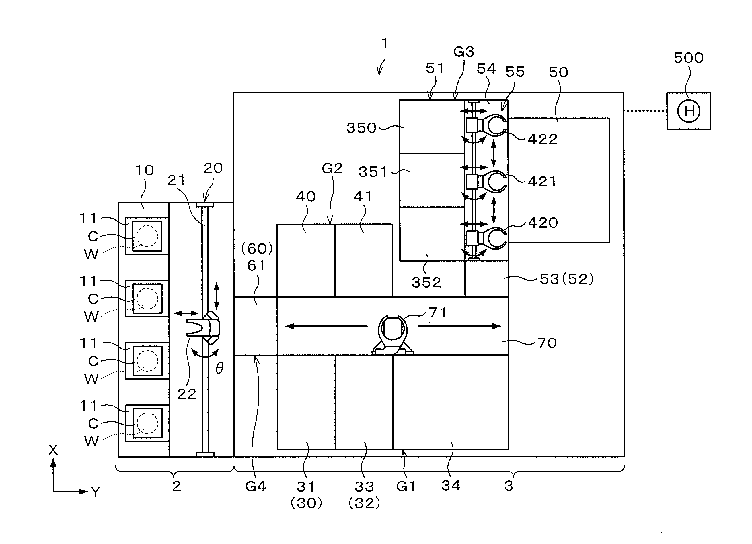
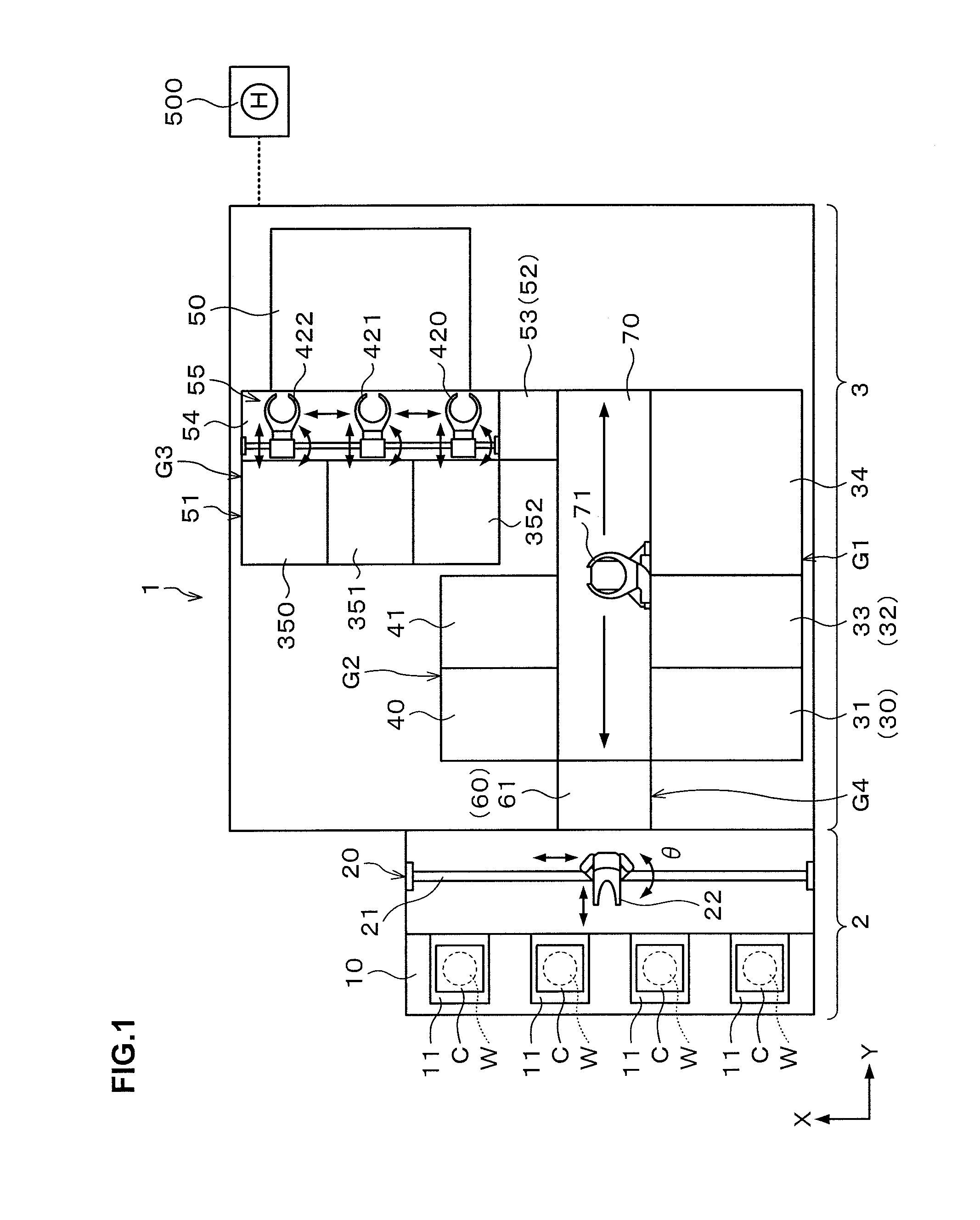
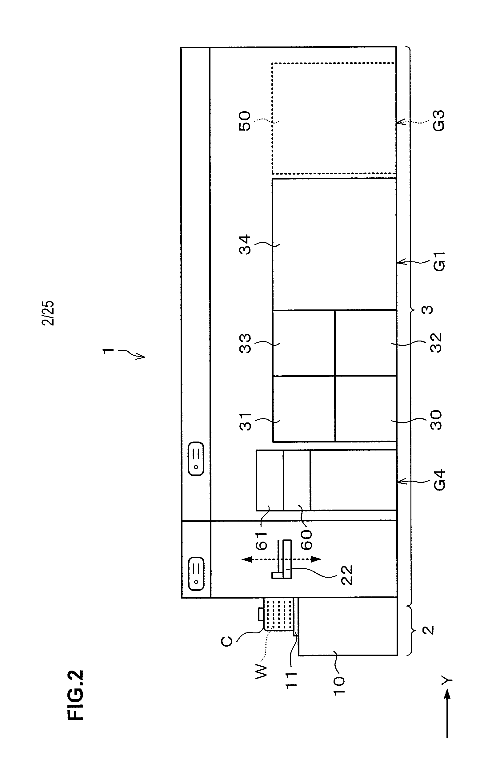
[0041]Hereinafter, an embodiment of the present invention will be described. FIG. 1 is a plan view illustrating the outline of configuration of a film forming system 1 according to this embodiment. FIG. 2 is a side view illustrating the outline of an internal configuration of the film forming system 1. Note that in this embodiment, a plurality of circuits have been formed on a front surface of a wafer as a substrate to be subjected to film forming treatment in the film forming system 1. Further, a coating film is formed on the wafer to seal the circuits in the film forming system 1.

[0042]The film forming system 1 has, as illustrated in FIG. 1, a configuration in which, for example, a transfer-in / out station 2 which a cassette C capable of housing a plurality of wafers W is transferred in / out from / to, for example, the outside, and a treatment station 3 including various treatment apparatuses that perform predetermined treatments on the wafers W, are integrally connected.

[0043]In the ...


PUM


Abstract

A film forming system includes a grinding apparatus that grinds a coating film on a front surface of a substrate, a cleaning apparatus that cleans the substrate from which the coating film has been ground, and a transfer apparatus that transfers the substrate. The cleaning apparatus includes a front surface cleaning unit that cleans the front surface of the substrate, and a rear surface cleaning unit that cleans a rear surface of the substrate. The transfer apparatus includes a first transfer arm that transfers the substrate before grinding of the coating film in the grinding apparatus or the substrate after cleaning in the cleaning apparatus, and a second transfer arm that transfers the substrate after grinding of the coating film in the grinding apparatus and before cleaning in the cleaning apparatus, or the substrate cleaned in either the front surface cleaning unit or the rear surface cleaning unit.

Description

CROSS REFERENCE TO RELATED APPLICATIONS[0001]This application is based upon and claims the benefit of priority of the prior Japanese Patent Application No. 2013-145296, filed in Japan on Jul. 11, 2013, and the prior Japanese Patent Application No. 2014-106082, filed in Japan on May 22, 2014, the entire contents of which are incorporated herein by reference.BACKGROUND OF THE INVENTION[0002]1. Field of the Invention[0003]The present invention relates to a film forming system for forming a coating film on a substrate having a plurality of circuits formed on a front surface thereof.[0004]2. Description of the Related Art[0005]For example, in a manufacturing process of a semiconductor device, after a plurality of circuits are formed on the front surface of a semiconductor wafer (hereinafter, referred to as a “wafer”), a so-called post process is performed. In the post-process, the wafer is cut into a plurality of semiconductor chips (hereinafter, referred to as “chips”) and then the chip...

Claims


Application Information

Patent Timeline
Patent Type & Authority Applications(United States)
IPC IPC(8): B05C21/00
CPCB05C21/00H01L21/67103H01L21/67051H01L21/67092H01L21/6715H01L21/67167
Inventor TERADA, TAKASHIHARA, SHOGO
Owner TOKYO ELECTRON LTD
Why Eureka
Try Eureka