
High-Purity Copper Sputtering Target

a high-purity, copper technology, applied in the direction of electrolysis components, vacuum evaporation coatings, coatings, etc., can solve the problems of affecting the uniformity of film thickness, affecting the utilization efficiency of target thereby deteriorating, and high input power of sputtering, so as to improve the strength of flange parts, improve the uniformity, and improve the effect of yield stress

Active Publication Date: 2014-12-18
JX NIPPON MINING & METALS CO LTD
View PDF1 Cites 5 Cited by
  • Summary
  • Abstract
  • Description
  • Claims
  • Application Information

AI Technical Summary

Benefits of technology

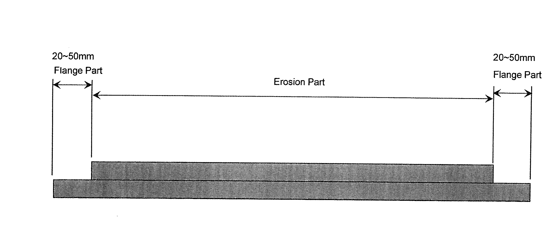
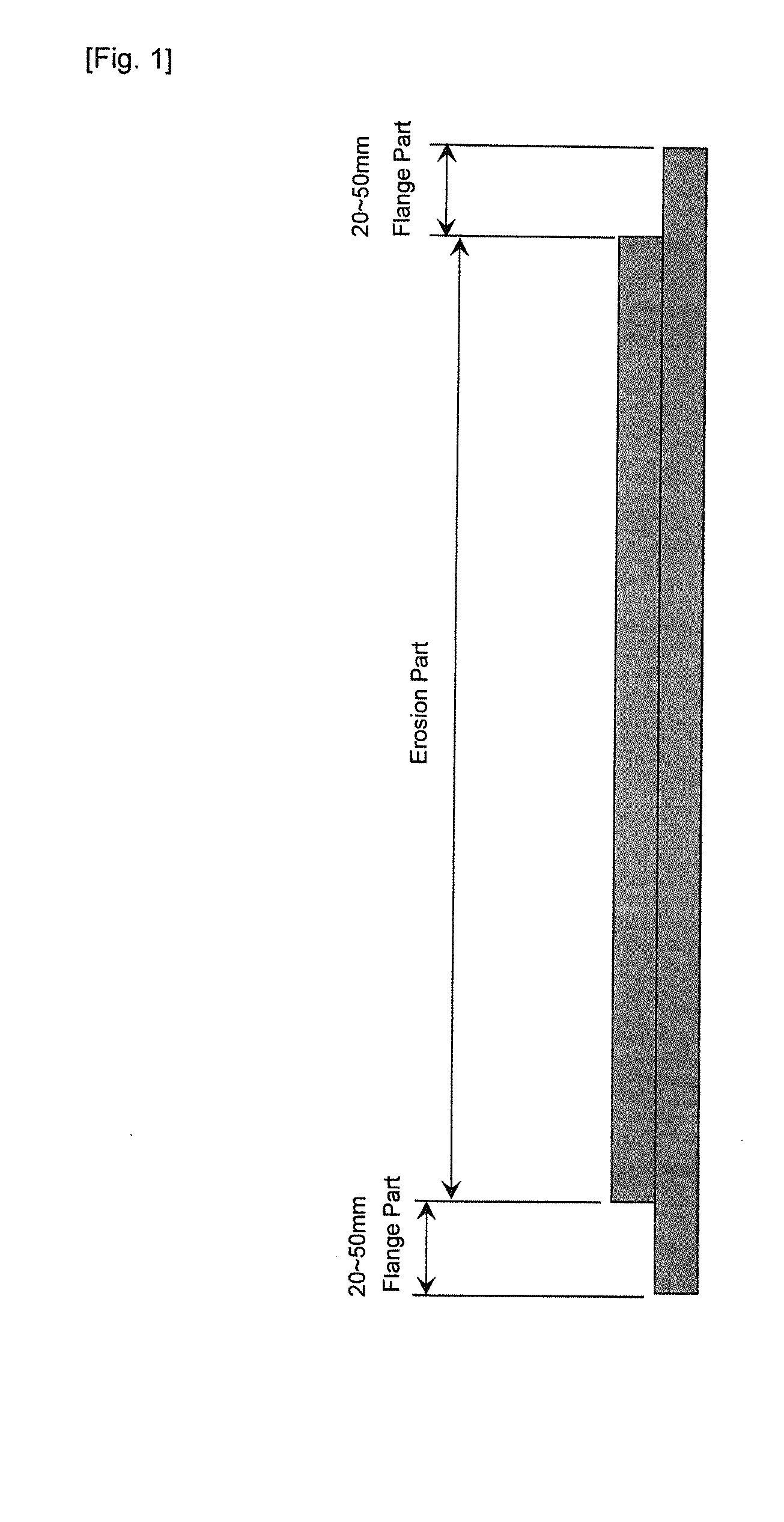
The present invention provides a high-purity copper sputtering target that is not bonded to a backing plate and has improved strength and reduced warping, resulting in a more uniform thin film. The target has a unique flange part that enhances the strength of the target. Additionally, the patent discusses an integrated target that can be easily recycled and is economically advantageous. This target improves the yield and reliability of semiconductor products and is useful for forming copper alloy wiring for semiconductors.

Problems solved by technology

Nevertheless, the input power of sputtering is extremely high in recent years, and the problem of deformation is being pointed out.
Thus, while the amount of deformation can be suppressed, due to the existence of the BP, the target needs to be formed thinner by that much, and the utilization efficiency of the target will thereby deteriorate.
Nevertheless, with this method, there is a problem in that the main orientation of the sputtering part of the target will also be the (220) orientation that has strain, and this affects the film thickness uniformity.
In the foregoing case, since Patent Document 2 is based on the premise of the integration of the target and the backing plate, inferiority in terms of conventional utilization efficiency is inevitable.
In the foregoing case, since Patent Document 3 is based on the premise of the integration of the target and the backing plate, inferiority in terms of conventional utilization efficiency is inevitable.
Nevertheless, there is no conventional technology that has developed a high-purity copper sputtering target material with the intent of suppressing the deformation of the target without using a backing plate, and improving the utilization efficiency of the target.

Method used


Image

  • High-Purity Copper Sputtering Target
  • High-Purity Copper Sputtering Target

Examples


example 1

[0042]High-purity copper (Cu) of purity 6N was melted in a high vacuum atmosphere using a carbon crucible. Molten metal of the copper was casted into a carbon mold in a high vacuum atmosphere to obtain an ingot. Subsequently, the produced ingot was subject to warm forging at 400° C. Subsequently, after a required amount was cut, the cut part was subject to rolling (cold working ratio of 82%) to attain a size of 530 (diameter)×30 (thickness), subject to heat treatment at 300° C. for 1 hour, and a range of 20 mm from the outer periphery was thereafter subject to cold forging (working ratio of 50%).

[0043]Subsequently, the obtained product was machined and processed into a target having a target part diameter of 430 mm, and a total thickness of 25 mm. Consequently, the target part had a recrystallized structure of roughly 35 μm, and the flange part became a worked structure based on cold working. In the foregoing case, since the flange part is of a worked structure, the crystal grain si...

example 2

[0048]High-purity copper (Cu) of purity 6N was melted in a high vacuum atmosphere using a carbon crucible. Molten metal of the copper was casted into a carbon mold in a high vacuum atmosphere to obtain an ingot.

[0049]Subsequently, the produced ingot was subject to warm forging at 400° C. Subsequently, after a required amount was cut, the cut part was subject to rolling (cold working ratio of 80%) to attain a size of 530 (diameter)×30 (thickness), subject to heat treatment at 325° C. for 1 hour, and a range of 30 mm from the outer periphery was thereafter subject to cold forging (working ratio of 40%). Subsequently, the obtained product was machined and processed into a target having a target part diameter of 430 mm, and a total thickness of 25 mm.

[0050]With regard to the high-purity copper sputtering target produced as described above, the hardness (Vickers hardness Hv) of the flange part, the (111) orientation ratio (%) of the erosion part, and the crystal grain size (μm) were exam...

example 3

[0054]High-purity copper (Cu) of purity 6N was melted in a high vacuum atmosphere using a carbon crucible. Molten metal of the copper was casted into a carbon mold in a high vacuum atmosphere to obtain an ingot. Subsequently, the produced ingot was subject to warm forging at 400° C. Subsequently, after a required amount was cut, the cut part was subject to rolling (cold working ratio of 80%) to attain a size of 530 (diameter)×30 (thickness), subject to heat treatment at 325° C. for 1 hour, and a range of 40 mm from the outer periphery was thereafter subject to cold forging (working ratio of 40%). Subsequently, the obtained product was machined and processed into a target having a target part diameter of 430 mm, and a total thickness of 25 mm.

[0055]With regard to the high-purity copper sputtering target produced as described above, the hardness (Vickers hardness Hv) of the flange part, the (111) orientation ratio (%) of the erosion part, and the crystal grain size (μm) were examined....


PUM

PropertyMeasurementUnit
crystal grain sizeaaaaaaaaaa
diameteraaaaaaaaaa
yield strengthaaaaaaaaaa

Abstract

A high-purity copper sputtering target, wherein a Vickers hardness of a flange part of the target is in a range of 90 to 100 Hv, a Vickers hardness of an erosion part in the central area of the target is in a range of 55 to 70 Hv, and a crystal grain size of the erosion part is 80 μm or less. This invention relates to a high-purity copper sputtering target that does not need to be bonded to a backing plate (BP), and aims to provide a high-purity copper sputtering target capable of forming a thin film having superior uniformity by enhancing a strength (hardness) of the flange part of the target, and reducing an amount of warpage of the target. Moreover, the uniformity of the film thickness is improved by adjusting the (111) orientation ratio of the erosion part and the flange part in the target. The present invention thereby aims to provide a high-purity copper sputtering target, which is capable of improving the yield and reliability of semiconductor products that are being subject to further miniaturization and higher integration, and useful for forming a copper alloy wiring for semiconductors.

Description

TECHNICAL FIELD[0001]The present invention provides a high-purity copper sputtering target with minimal deformation during sputtering and high utilization efficiency, and in particular relates to a high-purity copper sputtering target which is useful for forming a copper alloy wiring for semiconductors.BACKGROUND ART[0002]Conventionally, while an Al alloy (specific resistance of roughly 3.0 μΩ·cm) has been used as the wiring material of a semiconductor device, pursuant to the miniaturization of wirings, a copper wiring with lower resistance (specific resistance of roughly 2.0 μΩ·cm) has been put into practical application. As the process for forming a copper wiring, generally adopted is the method of forming a diffusion barrier layer made of Ta or TaN on a wiring or a wiring groove, and thereafter subjecting copper to sputter deposition. High-purity copper of 5N to 6N is normally produced by performing wet or dry purification to electrolytic copper having a purity level of 4N (exclu...

Claims


Application Information

Patent Timeline
Patent Type & Authority Applications(United States)
IPC IPC(8): H01J37/34
CPCH01J37/3426C23C14/3414C22C9/00C22F1/08
Inventor OKABE, TAKEOOTSUKI, TOMIOWATANABE, SHIGERU
Owner JX NIPPON MINING & METALS CO LTD
Learn More