
Electron emission element and method for manufacturing the same

a technology of electron emission element and manufacturing method, which is applied in the manufacture of electric discharge tube/lamp, discharge tube main electrode, and electric discharge system, etc. it can solve the problems of large power consumption, difficult to form x-ray tube in a small size, and high production cost, so as to achieve the effect of ensuring stability

Inactive Publication Date: 2014-10-02
INTELLECTUAL DISCOVERY CO LTD
View PDF6 Cites 2 Cited by
  • Summary
  • Abstract
  • Description
  • Claims
  • Application Information

AI Technical Summary

Benefits of technology

The patent text suggests that using a resin substrate can generate enough X-rays and provide stability while driving for a long time.

Problems solved by technology

Conventionally, an X-ray tube using a thermal electron emission source such as a tungsten filament has been widely used, but a much production cost is required, operation is performed in a high temperature condition, and power consumption is large.
Particularly, because upon applying as a micro focusing X-ray electron source, it is difficult to form the X-ray tube in a small size and the X-ray tube is less used due to a short life-span.
In such a structure, because of multi-layered structural characteristics, the structure has large contact resistance, thereby the large contact resistance becomes a cause that reduces a voltage supply for electron emission and therefore when the X-ray tube operates in a high pressure for a long time, a much heat occurs and adhesion is thus deteriorated.
Therefore, important characteristics of a threshold voltage, a maximum emission current, reliability, and a life-span are deteriorated.

Method used


Image

  • Electron emission element and method for manufacturing the same
  • Electron emission element and method for manufacturing the same
  • Electron emission element and method for manufacturing the same

Examples


experimental example

[0048]A substrate was prepared. After carbon nano tubes of 25 mg were added to sulfuric acid of 10 ml and nitric acid of 10 ml, the carbon nano tubes were distributed for 1 hour using an ultrasonic wave distribution device. By mixing and filtering sulfuric acid and nitric acid to which the carbon nano tubes were added for 15 hours using a mixer, refined carbon nano tubes were obtained. Next, after injecting the carbon nano tubes into refining water of 50 ml and SDS of 30 mg and by distributing the carbon nano tubes with an ultrasonic wave distribution device during 30 minutes, a suspension in which the carbon nano tubes were well-distributed was produced. The substrate was dipped in the previously produced suspension.

[0049]FIG. 4 is a photograph illustrating an apparatus for forming carbon nano tubes on a substrate in Experimental Example.

[0050]As shown in FIG. 4, by moving a substrate using a controller and a motor, the substrate is dipped in a suspension that is positioned at a lo...

experimental example 1

[0052]FIG. 5 is a scanning electron microscope photograph of a substrate surface that is used in Experimental Example 1.

[0053]As shown in FIG. 5, in Experimental Example 1, a resin substrate that is made of cellulose was used. As shown in FIG. 5, it was confirmed that fiber strands having a size of several μm are randomly entangled at the resin substrate. By washing a resin substrate to which the carbon nano tubes were attached using refining water, a dispersant was removed. After the dispersant was removed, the resin substrate was dried. The rest of the processes were the same as those of the foregoing Experimental Example.

experimental example 2

[0054]A resin substrate that is made of cellulose was used. However, the substrate was not washed by refining water before drying the substrate. Electric field emission characteristics and stability of the electron emission device that is produced by the foregoing method were experimented. The rest of the processes were the same as those of the foregoing Experimental Example.


PUM

PropertyMeasurementUnit
surface roughness Raaaaaaaaaaa
diameteraaaaaaaaaa

Abstract

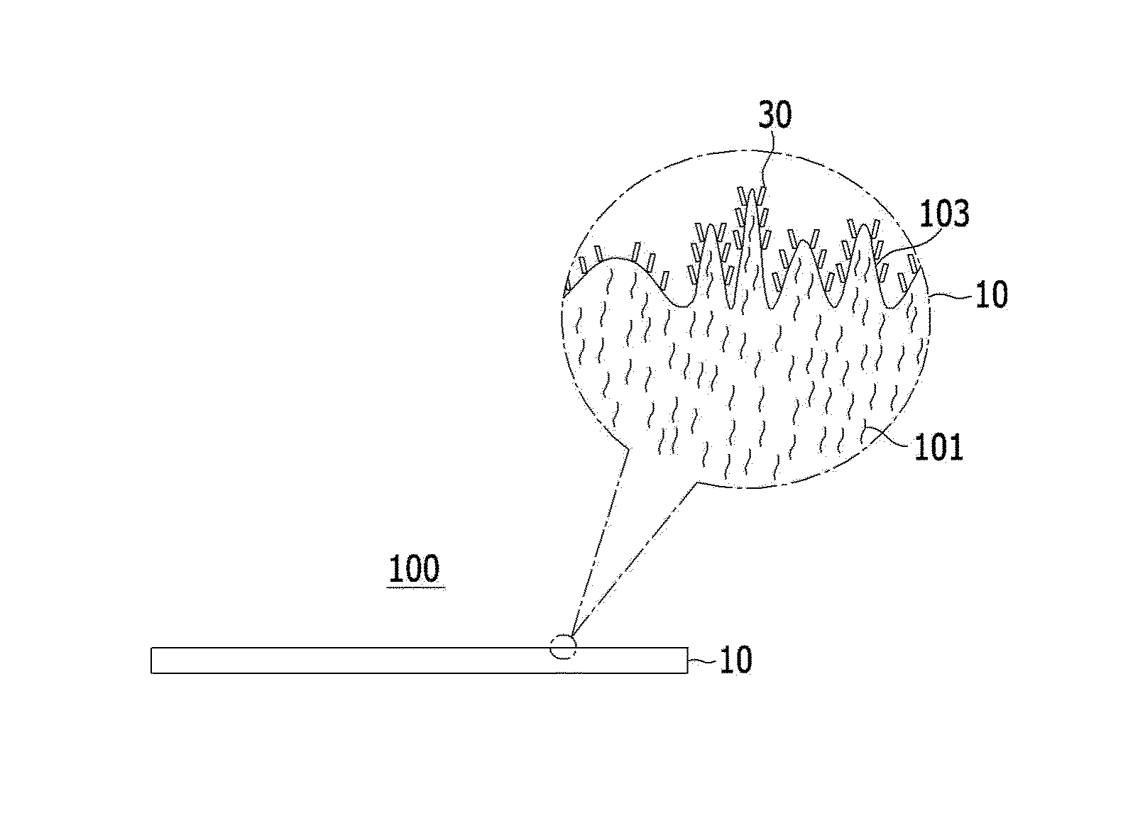
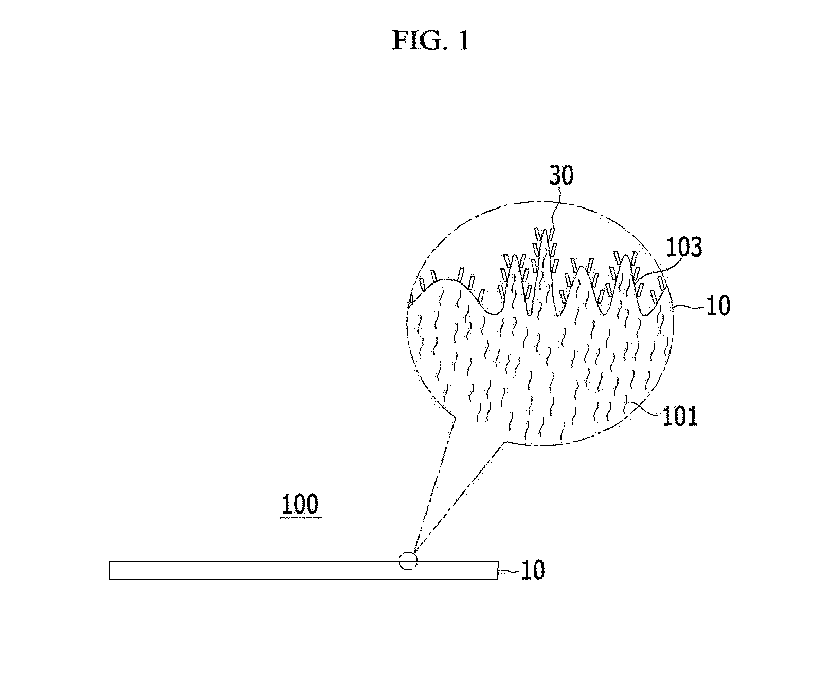
An electron emission device and a method of manufacturing the same are provided. The electron emission device includes i) a hydrophilic resin substrate and ii) carbon nano tubes that are positioned on the resin substrate. Surface roughness Ra of the resin substrate is 7.3 μm to 9.75 μm.

Description

CROSS-REFERENCE TO RELATED APPLICATION[0001]This application is related to Korean Patent Application No. 2013-0033108 that was filed in the Korean Industrial Property Office on Mar. 27, 2013, “Enhancement of electron-emission and long-term stability in tip-type carbon nanotube field emitters by lithium coating”, which is a material that was announced at the 39th ICMCTF on Apr. 23, 2012, and “Electric field emission characteristics of carbon nano tube emitter using cellulose substrate”, which is a material that was announced at the 43rd summer scientific contest of Korean electric society on Jul. 8, 2012.BACKGROUND OF THE INVENTION[0002](a) Field of the Invention[0003]The present invention relates to an electron emission device and a method of manufacturing the same. More particularly, the present invention relates to an electron emission device and a method of manufacturing the same that embody a high current density and a high electron emission degree by adjusting average surface r...

Claims


Application Information

Patent Timeline
Patent Type & Authority Applications(United States)
IPC IPC(8): H01J9/02H01J1/304
CPCH01J1/3042B82Y30/00H01J9/025H01J2201/30434H01J2329/861H01J2329/0431H01J2329/8615H01J2201/30469H01J1/304H01J9/02
Inventor PARK, JIN SEOKKIM, BU JONGKIM, WONLEE, SANG HYUK
Owner INTELLECTUAL DISCOVERY CO LTD
Learn More