
Ingot growing apparatus and method of manufacturing ingot

a growing apparatus and ingot technology, applied in the direction of polycrystalline material growth, crystal growth process, protective fluid, etc., can solve the problems of increased dislocation propagation velocity, 450 mm weight, and difficulty in removing dislocations in the neck portion, so as to reduce the dislocation propagation velocity and reduce the weight of the ingot that may be supported by the neck portion , the effect of increasing the weigh

Active Publication Date: 2014-07-10
LG SILTRON
View PDF3 Cites 0 Cited by
  • Summary
  • Abstract
  • Description
  • Claims
  • Application Information

AI Technical Summary

Benefits of technology

This patent describes an apparatus and method for manufacturing ingots of semiconductor materials. The apparatus includes a dopant supply unit that produces a high concentration of dopant in the neck portion of the ingot, which reduces dislocation propagation and shortens the propagation length. This helps to quickly control defects and prevents process failure. The diameter of the neck portion is increased, allowing a heavy weight ingot to be supported, resulting in a high-quality, large diameter wafer. Overall, this invention improves the manufacturing process and yield of semiconductor materials.

Problems solved by technology

However, since the generated shear stress increases as the diameter of the neck portion increases, the dislocation propagation velocity is more increased, and thus, it is difficult to remove dislocations in the neck portion having a diameter of 5 mm or more by simply increasing the crystal growth rate of the neck portion.
However, it is estimated that a weight of a 450 mm crystal in the future may reach about 1 ton and it is impossible to support the heavy weight (>500 kg) of the 450 mm crystal by using the present process of forming a neck portion having a diameter of about 5 mm.

Method used


Image

  • Ingot growing apparatus and method of manufacturing ingot
  • Ingot growing apparatus and method of manufacturing ingot
  • Ingot growing apparatus and method of manufacturing ingot

Examples


Embodiment Construction

Mode for the Invention

[0025]In the description of embodiments, it will be understood that when a layer (or film), region, pattern or structure is referred to as being ‘on / over’ or ‘under / below’ another layer (or film), region, pad or pattern, it can be directly on the other layer or substrate, or intervening layers may also be present. Further, the reference about ‘on / over’ or ‘under / below’ each layer will be made on the basis of drawings.

[0026]In the drawings, the thickness or size of each layer (or film), region, pattern or structure may be modified for convenience in description and clarity, and does not entirely reflect an actual size.

[0027]Hereinafter, embodiments of the present invention will be described in detail with reference to the accompanying drawings.

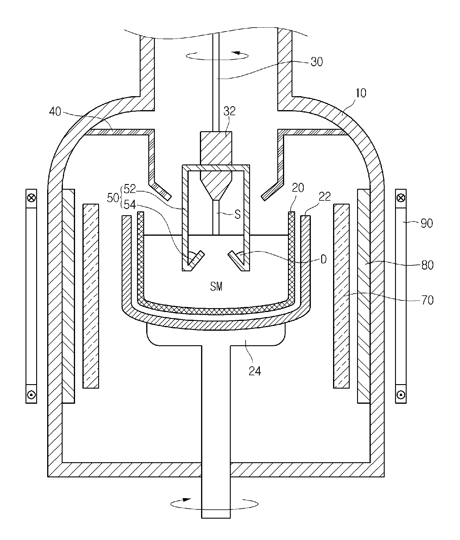
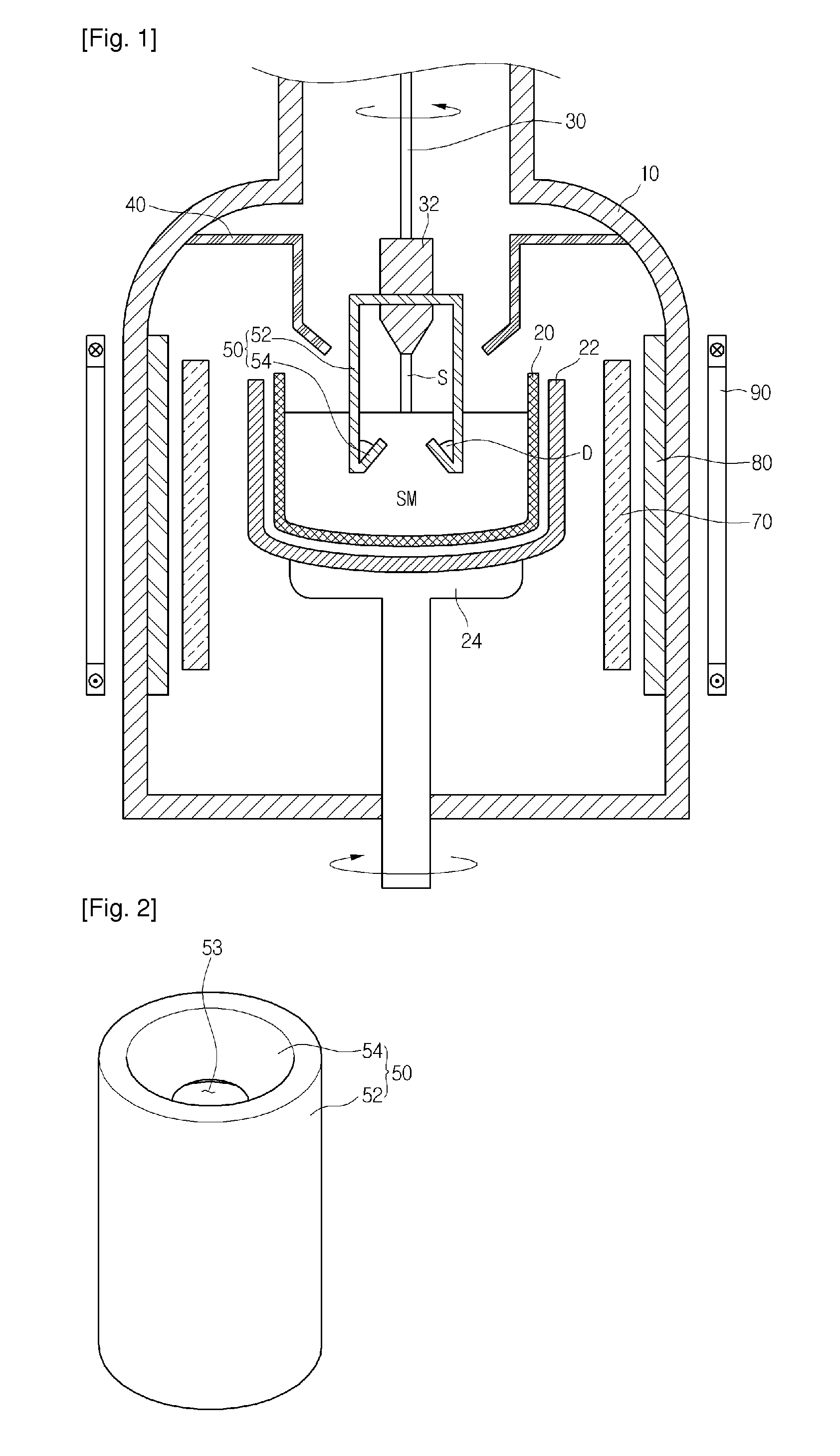
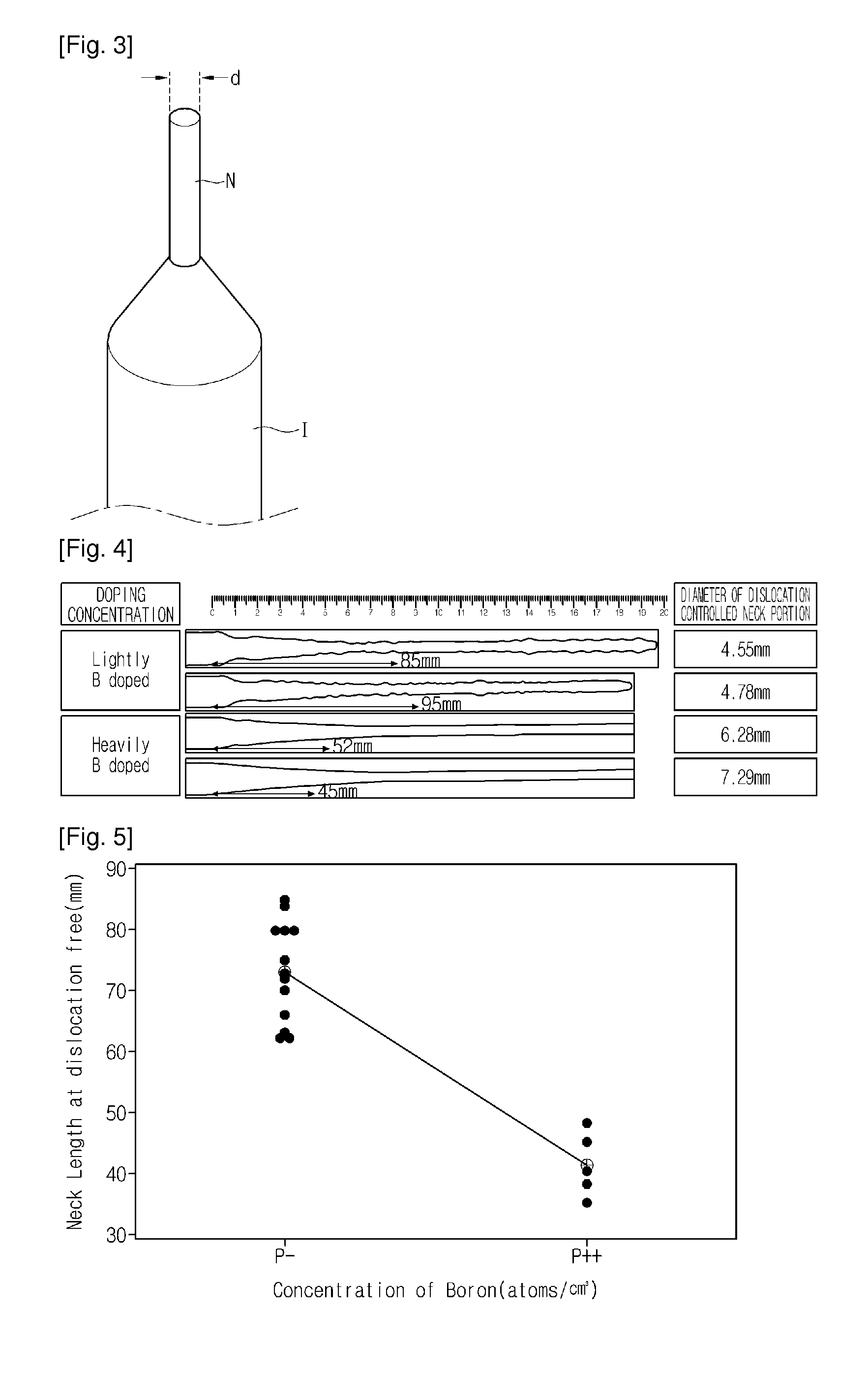
[0028]A silicon single crystal ingot manufacturing apparatus according to an embodiment is described in detail with reference to FIGS. 1 through 7. FIG. 1 is a cross-sectional view illustrating an ingot manufacturing appar...


PUM

PropertyMeasurementUnit
diameteraaaaaaaaaa
diameteraaaaaaaaaa
weightaaaaaaaaaa

Abstract

Provided is an ingot growing apparatus, which includes a crucible containing a silicon melt, a pulling device pulling a silicon single crystal ingot grown from the silicon melt, and a dopant supply unit disposed adjacent to the pulling device and for supplying a dopant during growing of the ingot. The neck portion may be doped at a concentration higher than that of the ingot through the dopant supply unit. Therefore, dislocation propagation velocity may be decreased and a propagation length may be shortened.

Description

CROSS-REFERENCE TO RELATED APPLICATIONS[0001]The present application is a national phase application of P.C.T. application PCT / KR2012 / 006415 filed Aug. 10, 2012, which claims the priority benefit of Korean patent application 10-2011-0080639 filed Aug. 12, 2011, the disclosures of which are incorporated herein by reference.BACKGROUND OF THE INVENTION[0002]1. Field of the Invention[0003]The present disclosure relates to an ingot growing apparatus and a method of manufacturing an ingot.[0004]2. Description of the Related Art[0005]In general, a process of manufacturing a wafer for fabricating a semiconductor device may include a cutting process slicing a silicon single crystal ingot, an edge grinding process rounding an edge of the sliced wafer, a lapping process planarizing a rough surface of the wafer due to the cutting process, a cleaning process removing various contaminants including particles adhered to the surface of the wafer during the edge grinding or lapping process, a surfac...

Claims


Application Information

Patent Timeline
Patent Type & Authority Applications(United States)
IPC IPC(8): C30B15/04
CPCC30B29/06C30B15/32C30B15/04Y10T117/1032H01L21/02
Inventor AHN, JIN-WOOKIM, BONG-WOOCHOI, IL-SOOKIM, DO-YEON
Owner LG SILTRON
Learn More