Adjustable non-dissipative voltage boosting snubber network

a non-dissipative, voltage-boosting technology, applied in the direction of electric variable regulation, process and machine control, instruments, etc., can solve the problems of reducing affecting the efficiency of power dissipation, so as to achieve the effect of boosting a voltage and reducing the voltag

Active Publication Date: 2014-05-01
AES GLOBAL HLDG PTE LTD
View PDF0 Cites 59 Cited by
  • Summary
  • Abstract
  • Description
  • Claims
  • Application Information

AI Technical Summary

Benefits of technology

The disclosure is about a circuit called a snubber circuit that helps to reduce voltage spikes and protect electronic components. It consists of a voltage multiplier, a current-limiter, and a unidirectional switch. The voltage multiplier increases the voltage between two power rails, and then decreases it again. The current-limiter provides a low-resistance path for current to flow from the voltage multiplier to the first power rail while limiting the rate at which current changes. The unidirectional switch allows current to flow from one power rail to the voltage multiplier, but blocks it from flowing back again. Overall, this circuit helps to protect electronic components from voltage spikes and allows for smoother operation.

Problems solved by technology

Instead, the power predominantly passes through the switching circuit 104 potentially damaging the switching circuit 104.
Additional challenges to known power supply systems include slow processing throughput and further inefficiencies from power dissipation.
This leads to longer processing periods and decreased throughput, since many processes can only end when a predetermined total power has been delivered.
Furthermore, since each pulse is shorter at higher frequency, the current at high frequency may end up larger (in a power-regulated system) than at lower frequency.
Since power dissipation is proportional to I2, these larger currents lead to larger power losses.
Additionally, switching losses, which are proportional to the current at the moment of switching, are accentuated at higher frequencies since switching current is larger.

Method used


Image

  • Adjustable non-dissipative voltage boosting snubber network
  • Adjustable non-dissipative voltage boosting snubber network
  • Adjustable non-dissipative voltage boosting snubber network

Examples


Embodiment Construction

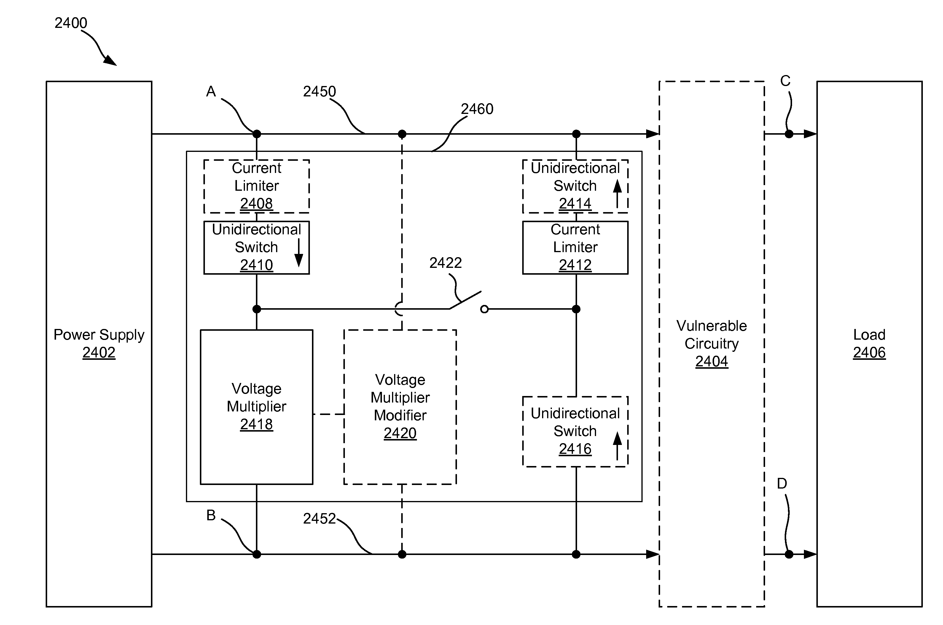
[0038]The present disclosure relates generally to power supply systems. More specifically, but without limitation, the present disclosure relates to a non-dissipative snubber for use in a power supply system.

[0039]The word “exemplary” is used herein to mean “serving as an example, instance, or illustration.” Any embodiment described herein as “exemplary” is not necessarily to be construed as preferred or advantageous over other embodiments.

[0040]For the purposes of this disclosure, a current limiter is any device or circuit that limits a current that can pass through the current limiter or that limits a rate at which current passing through the current limiter can rise or fall. In some embodiments, a current limiter can limit both the rate of increase and an upper bound of the current passing through the current limiter. An inductor, resistor, JFET, MOSFET, and IGBT are all examples of current-limiting elements since each are able to limit the rate of change of and amount of current...


PUM


Abstract

This disclosure describes a non-dissipative snubber circuit configured to boost a voltage applied to a load after the load's impedance rises rapidly. The voltage boost can thereby cause more rapid current ramping after a decrease in power delivery to the load which results from the load impedance rise. In particular, the snubber can comprise a combination of a unidirectional switch, a voltage multiplier, and a current limiter. In some cases, these components can be a diode, voltage doubler, and an inductor, respectively.

Description

FIELD OF THE DISCLOSURE[0001]The present disclosure relates generally to power supplies. In particular, but not by way of limitation, the present disclosure relates to systems, methods and apparatuses for limiting voltage and current spikes in a power supply.BACKGROUND[0002]FIG. 1 illustrates one example of a typical power supply system 100 used for plasma processing. The power supply system 100 includes a DC power supply 102 providing DC power to a switching circuit 104 that converts the DC power into pulsed DC and provides the pulsed DC to a plasma load 106. When switching, the potential between nodes C and D passes through a potential of zero, and the plasma can be extinguished or can dim to an extent that it becomes highly resistive and acts like an unfluxed inductor or an open circuit for a short time after this transition. Immediately after this transition, the DC power supply 102 continues to provide power to the switching circuit 104, but most of that power can no longer be ...

Claims


Application Information

Patent Timeline
IPC IPC(8): H02H9/00G05F1/46H05H1/48
CPCH02H9/00G05F1/46H05H1/48H01J37/3405H01J37/3444H05H1/46H02H9/042H05H2242/26H02H3/087
Inventor FINLEY, KENNETH W.
Owner AES GLOBAL HLDG PTE LTD
Why Eureka
Try Eureka