Heating and heat dissipating multi-layer circuit board structure for keeping operating temperature of electronic components
- Summary
- Abstract
- Description
- Claims
- Application Information
AI Technical Summary
Benefits of technology
Problems solved by technology
Method used
Image
Examples
first embodiment
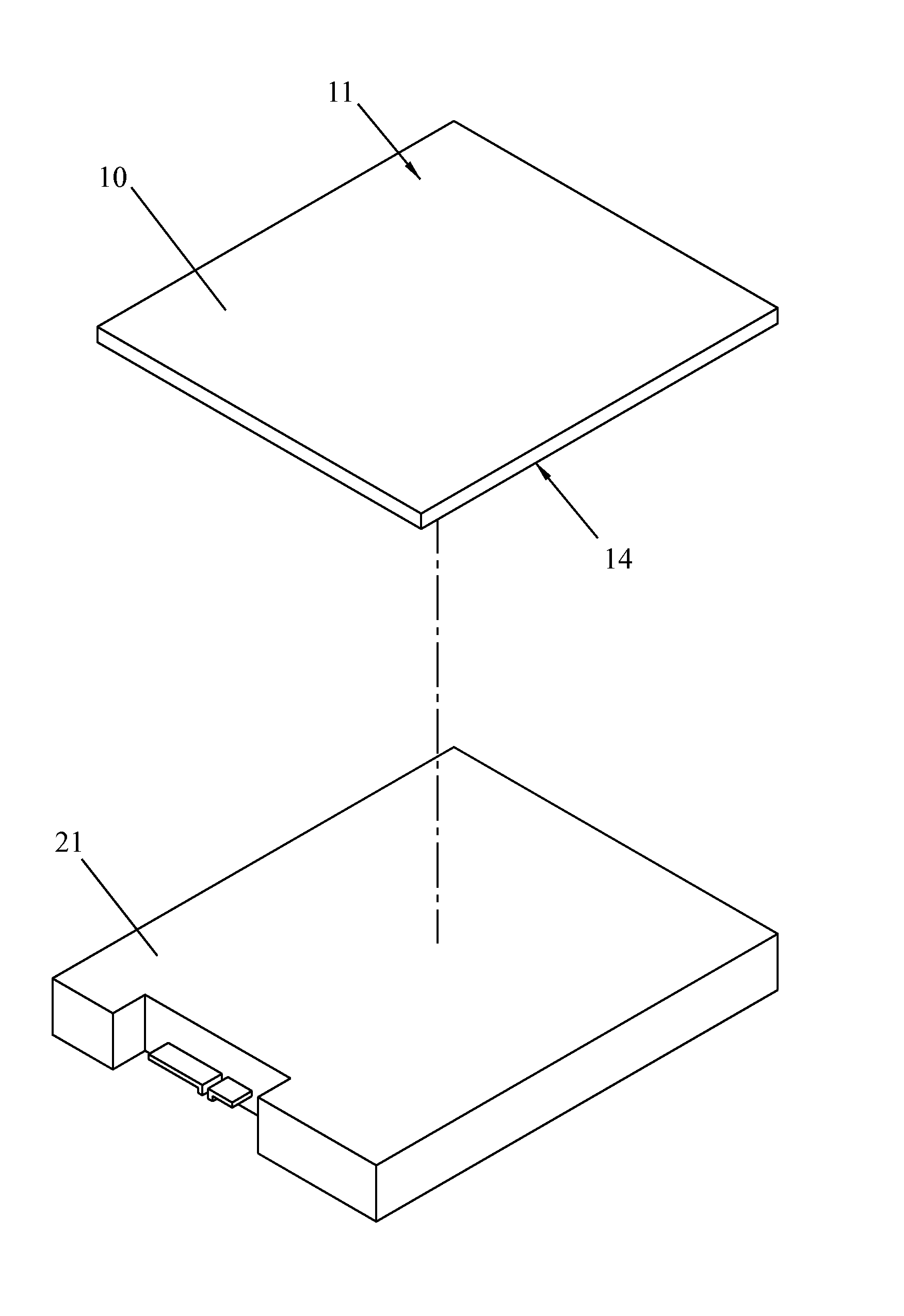
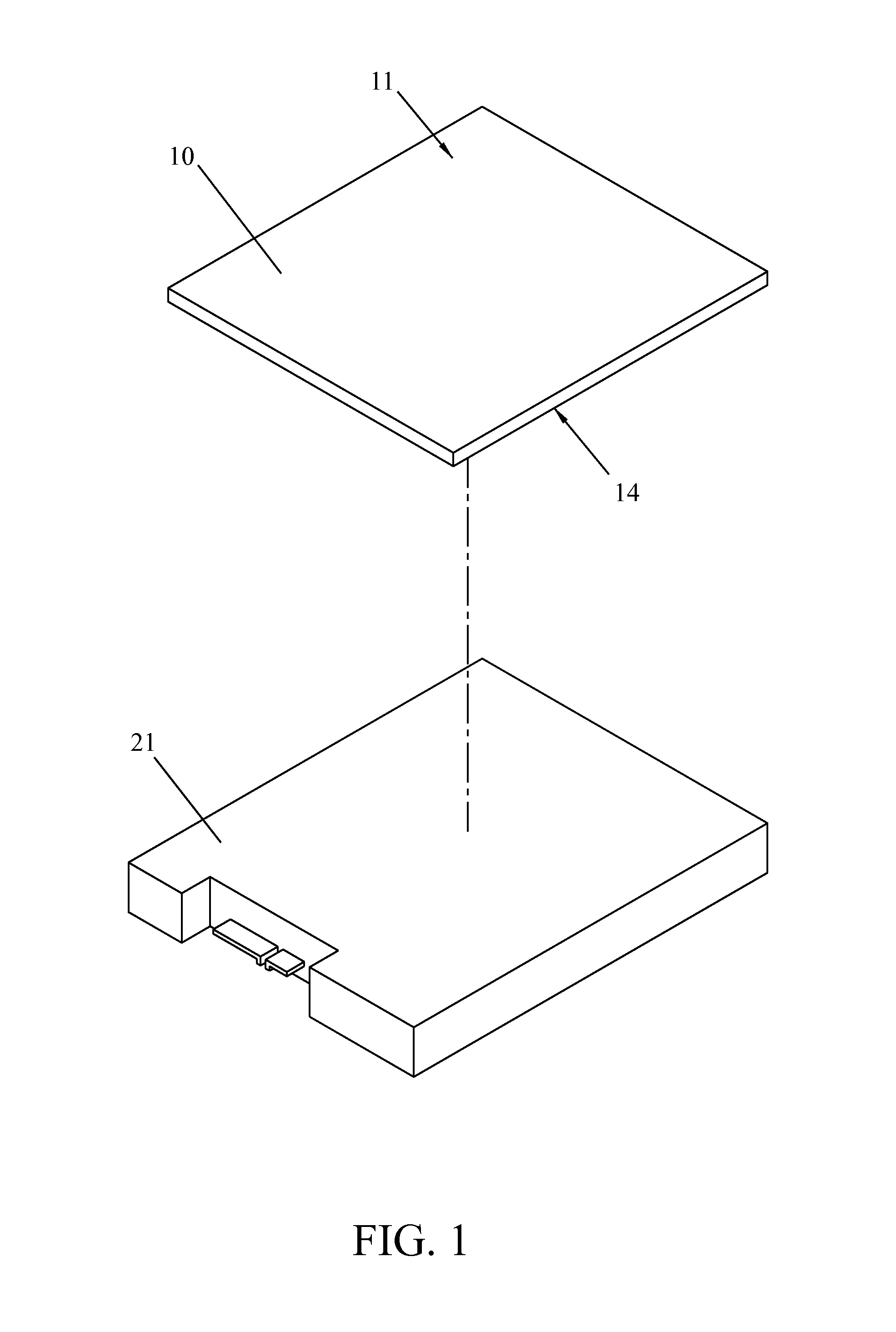
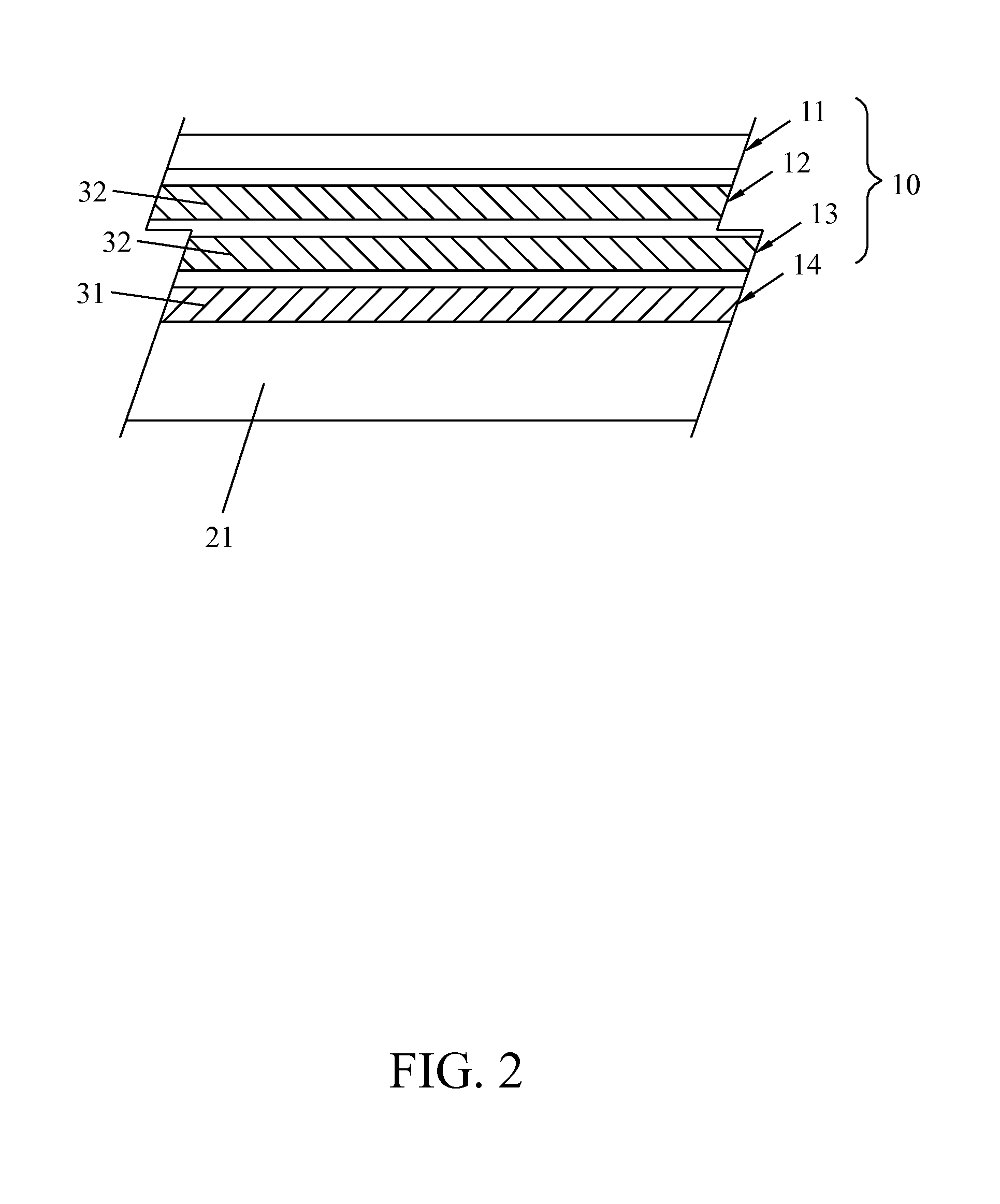
[0027]In the invention, the electronic component 21 is represented by a hard disk drive (HDD). The multi-layer PCB 10 is a four-layered PCB containing a first layer 11, a second layer 12, a third layer 13, and a fourth layer 14. The first layer 11 and the fourth layer 14 are the outer layers of the multi-layer PCB 10. The second layer 12 and the third layer 13 are the inner layers of the multi-layer PCB 10.
[0028]The electronic component 21 is in contact with the surface of the fourth layer 14 of the multi-layer PCB 10 by attaching in conjunction with other fixation methods (e.g., screwing). The power of the multi-layer PCB 10 and the electronic component 21 is provided by an external power source (not shown). For example, a motherboard provides the power of the multi-layer PCB 10 and the electronic component 21. Such a possibility is only an example, and should not be used to restrict the scope of the invention.
[0029]Please simultaneously refer to FIGS. 2 and 3. FIG. 3 is a planar v...
second embodiment
[0038]In the second embodiment, the first electronic component 51, the second electronic component 52, and the third electronic component 53 are chips as an example. The multi-layer PCB 40 is a six-layered PCB. The multi-layer PCB 40 includes a first layer 41, a second layer 42, a third layer 43, a fourth layer 44, a fifth layer 45 and a sixth layer 46. The first layer 41 and the sixth layer 46 are the outer layers of the multi-layer PCB 40. The second layer 42, the third layer 43, the fourth layer 44, and the fifth layer 45 are the inner layers of the multi-layer PCB 40.
[0039]The first electronic component 51 is welded to have surface contact with the first layer 41 of the multi-layer PCB 40. The second electronic component 52 and the third electronic component 53 are welded to have surface contacts with the sixth layer 46 of the multi-layer PCB 40. In the second embodiment, the multi-layer PCB 40 can be a motherboard or an extension board (e.g., display card, sound card, extension...
PUM
 Abstract
Description
Claims
Application Information
 - R&D
- Intellectual Property
- Life Sciences
- Materials
- Tech Scout
- Unparalleled Data Quality
- Higher Quality Content
- 60% Fewer Hallucinations
Browse by: Latest US Patents, China's latest patents, Technical Efficacy Thesaurus, Application Domain, Technology Topic, Popular Technical Reports.
© 2025 PatSnap. All rights reserved.Legal|Privacy policy|Modern Slavery Act Transparency Statement|Sitemap|About US| Contact US: help@patsnap.com


