
Digital switched mode voltage regulator

a voltage regulator and digital switch technology, applied in the direction of electrical variable regulation, efficient power electronics conversion, instruments, etc., can solve the problem that the integrated portion of the regulation loop may not be able to respond to small or moderate load fluctuations at the output voltage, and achieve the effect of improving loop stability, ensuring circuit complexity, and maintaining circuit complexity, area and power consumption at an acceptable level

Active Publication Date: 2014-01-02
ANALOG DEVICES INT UNLTD
View PDF2 Cites 27 Cited by
  • Summary
  • Abstract
  • Description
  • Claims
  • Application Information

AI Technical Summary

Benefits of technology

The patent describes a regulation loop for a switched mode voltage regulator circuit that can quickly respond to changes in load fluctuations at the output voltage. The regulation loop includes a linear digital filter and a non-linear digital filter, which work together to ensure a stable output voltage. The non-linear digital filter has a high gain operating at the desired output voltage, allowing it to respond to small changes in the load. The linear digital filter is designed to handle the linear portion of the regulation loop, while the non-linear digital filter ensures good steady-state tracking. The analog-to-digital converter used in the circuit has a high resolution flash A / D converter, which helps in stabilizing the regulation loop. The non-linear digital filter has a varying gain depending on the value of the digital error signal, which allows for a faster response to changes in load. The counter circuit is designed to adjust the gain of the non-linear digital filter based on the value of the digital error signal. The driver control signal can be modulated using both pulse width and pulse density modulation, depending on the level of the combined digital error signal.

Problems solved by technology

If the non-linear digital filter comprises a range of the digital error signal where the gain applied to the digital error signal is small or even zero, the integral portion of the regulation loop may be unable to respond to small or moderate load fluctuations at the output voltage.

Method used


Image

  • Digital switched mode voltage regulator
  • Digital switched mode voltage regulator
  • Digital switched mode voltage regulator

Examples


first embodiment

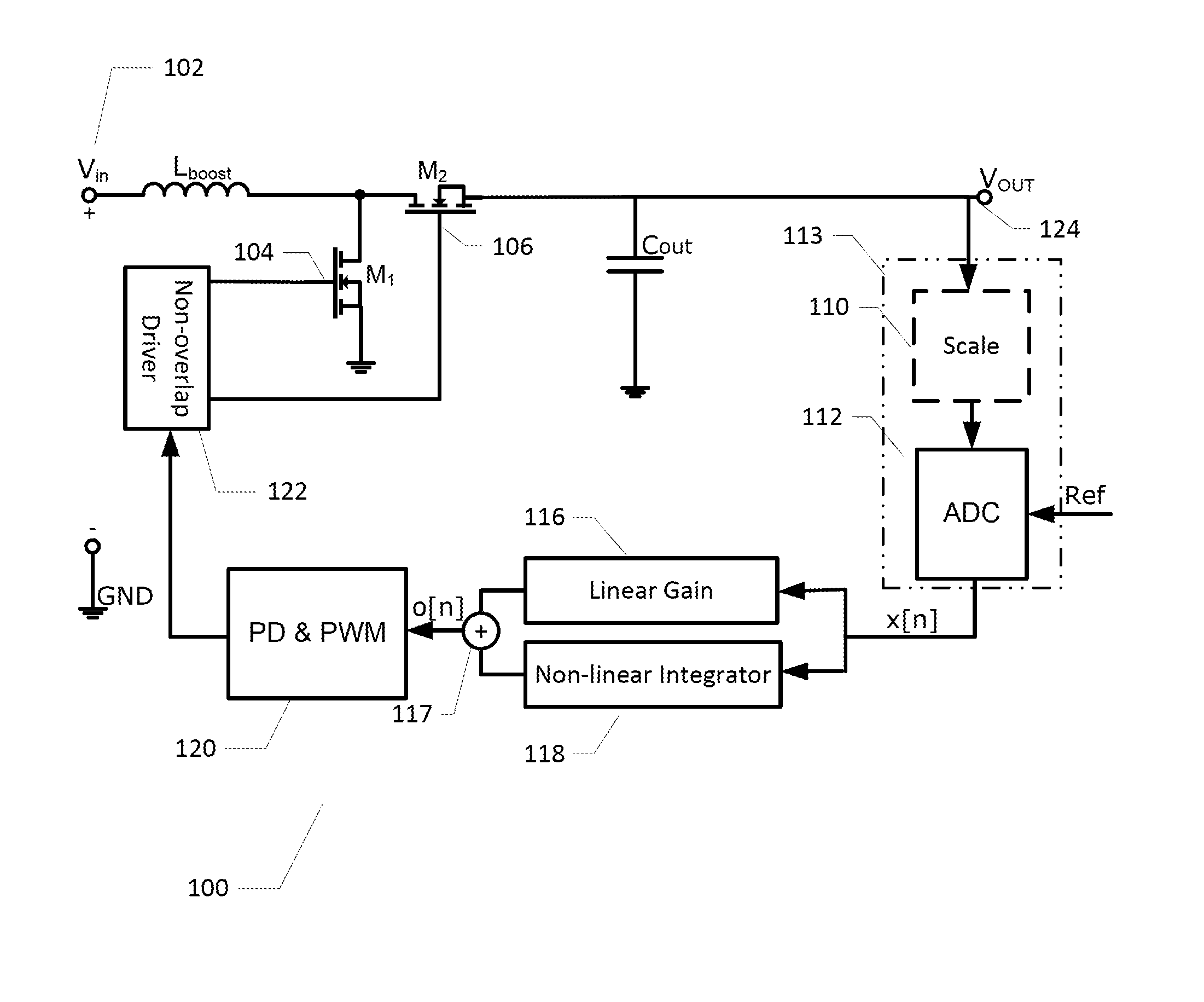
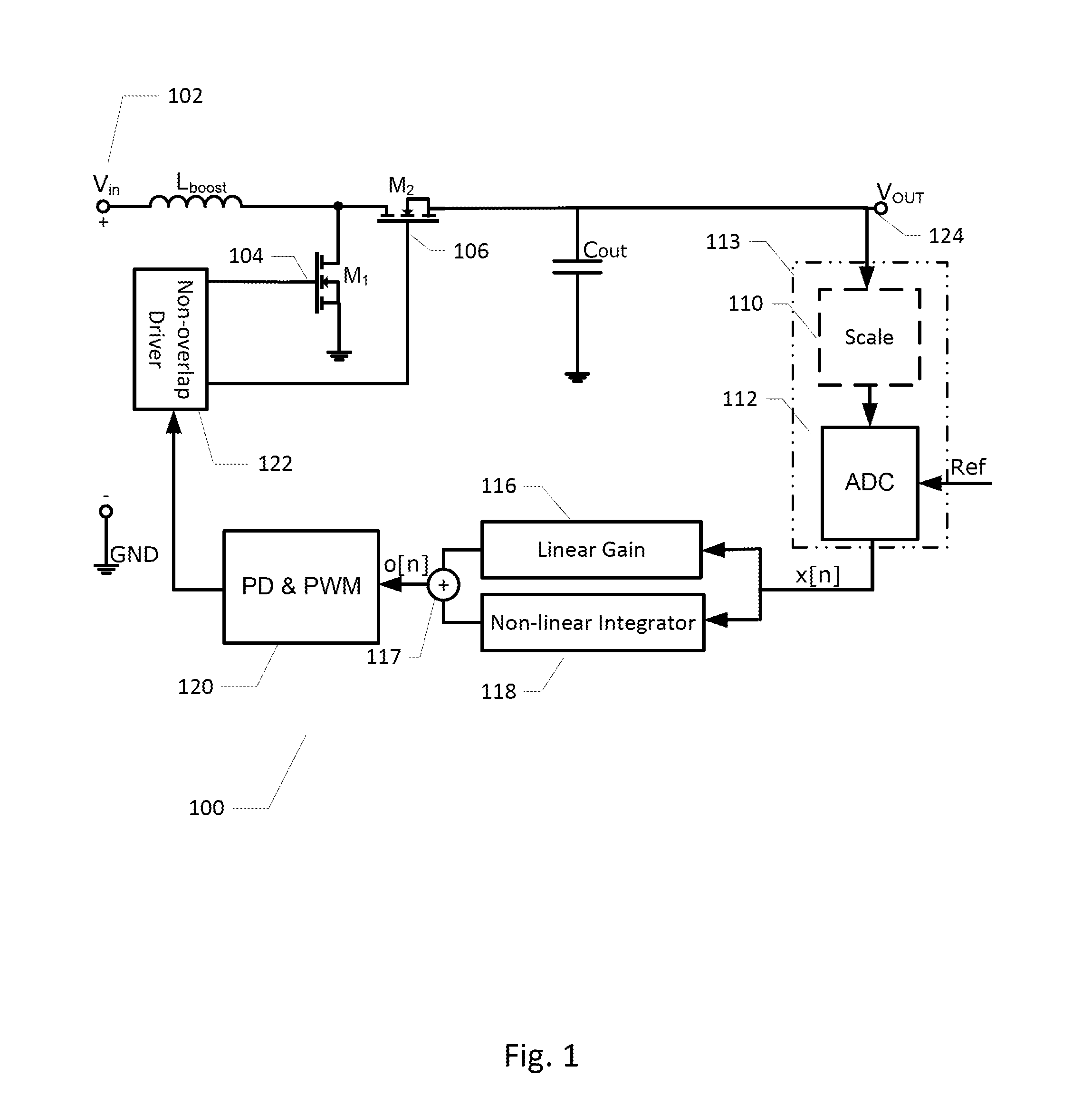
[0035]FIG. 1 illustrates schematically a boost-type of switched mode voltage regulator circuit 100 in accordance with the invention. The switched mode voltage regulator circuit 100 comprises an input terminal 102 for receipt of a regulator input voltage Vin for example a DC power rail or a DC voltage from a rechargeable battery. An output terminal 124 is electrically coupled to an output capacitor Cout for supply of a DC output voltage VOUT. A converter inductance is provided by an inductor Lboost which is electrically coupled to the regulator input voltage such that Lboost is charged with energy from Vin through a first semiconductor switch, formed by CMOS transistor M1, in a first regulator mode. In the first regular mode, the CMOS transistor M1 is placed in a conducting state or on-state by non-overlapping switch driver 122 by applying an appropriate gate voltage to gate terminal 104 of M1. The non-overlapping switch driver 122 furthermore places a second semiconductor switch, in...

second embodiment

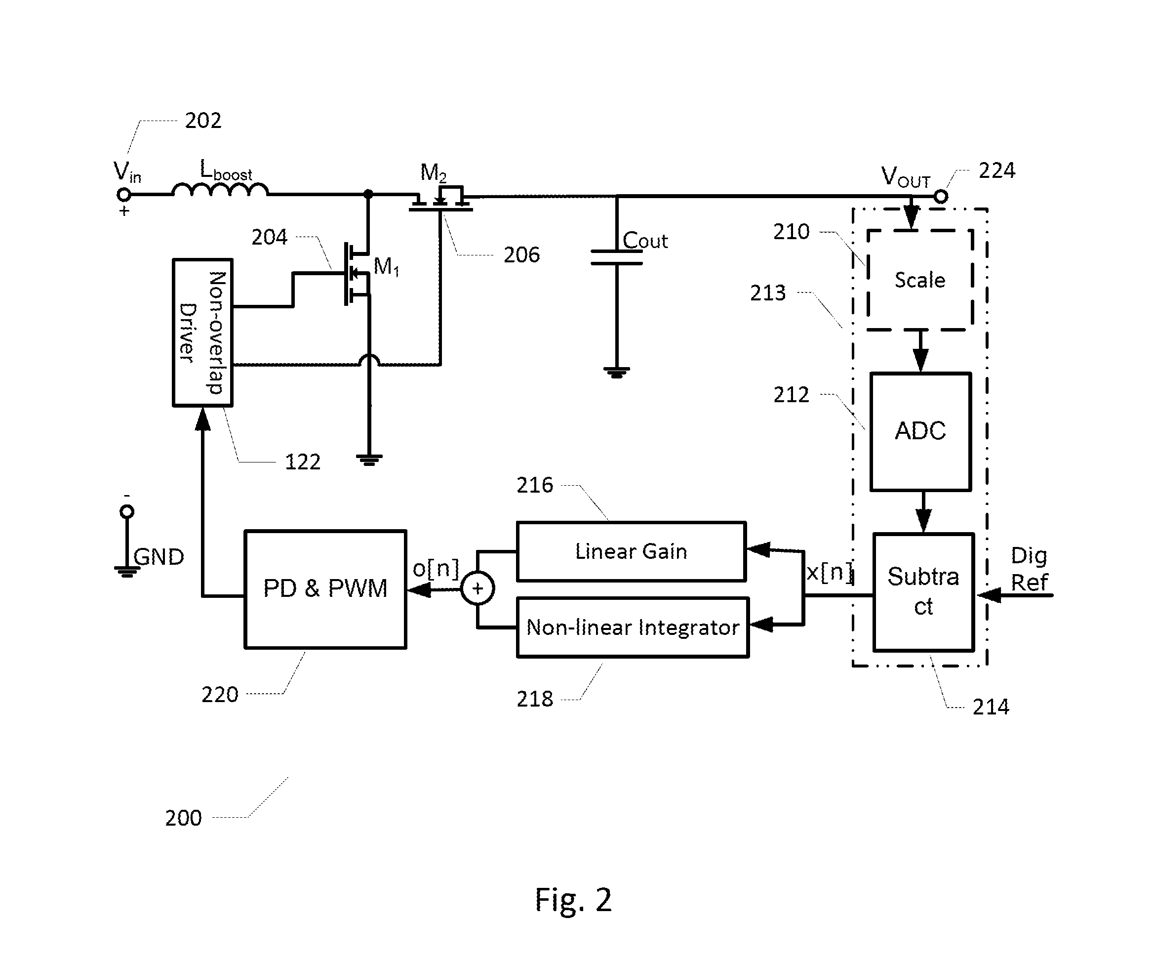
[0041]FIG. 2 illustrates schematically a boost-type of switched mode voltage regulator circuit 200 in accordance with the invention. The switched mode voltage regulator circuit 200 shares numerous features with the above described voltage regulator circuit 100 and corresponding features have been provided with corresponding reference numerals to assist comparison. The main difference is how the digital error signal x[n] is generated. In the present embodiment, the reference voltage is provided in digital representation, i.e. as a digital reference voltage or number, indicated by arrow “Dig Ref” to the error signal generator 213. An analog-to-digital converter 212, which may have similar characteristics to the above-discussed converter 112, is operatively coupled to the DC output voltage to provide a digital / digitized DC output voltage number or signal. The digitized DC output voltage signal is applied to a first input of a digital subtractor 214 while the digital reference voltage i...


PUM


Abstract

The present invention relates to a switched mode voltage regulator circuit comprising a regulation loop coupled between the output voltage of the regulator and a switch driver. The regulation loop comprising an error signal generator supplying a digital error signal representative of a voltage difference between the output voltage and a reference voltage. The regulation loop further comprises a linear digital filter and a non-linear digital filter both coupled for receipt of the digital error signal and a digital summer coupled for receipt of linearly and non-linearly filtered digital error signals to provide a combined digital error signal. A digital pulse modulator is configured to generate the pulse width or pulse density modulated driver control signal in accordance with the combined digital error signal.

Description

[0001]The present invention relates to a switched mode voltage regulator circuit comprising a regulation loop coupled between the output voltage of the regulator and a switch driver. The regulation loop comprising an error signal generator supplying a digital error signal representative of a voltage difference between the output voltage and a reference voltage. The regulation loop further comprises a linear digital filter and a non-linear digital filter both coupled for receipt of the digital error signal and a digital summer coupled for receipt of linearly and non-linearly filtered digital error signals to provide a combined digital error signal. A digital pulse modulator is configured to generate the pulse width or pulse density modulated driver control signal in accordance with the combined digital error signal.BACKGROUND OF THE INVENTION[0002]U.S. Pat. No. 7,952,337 discloses a hybrid switching voltage regulator of boost and / or buck topology. The voltage regulator comprises two ...

Claims


Application Information

Patent Timeline
Patent Type & Authority Applications(United States)
IPC IPC(8): G05F1/00
CPCH02M3/157H02M3/1588H02M1/0054Y02B70/10
Inventor WISMAR, ULRIK SORENSENGAADESTRUP, SOREN
Owner ANALOG DEVICES INT UNLTD
Learn More