
Monitoring method and apparatus for excimer laser annealing process

a laser annealing and monitoring method technology, applied in laser beam welding apparatus, crystal growth process, instruments, etc., can solve the problems of affecting the production line throughput of acceptable panels, and affecting the quality of the produ

Inactive Publication Date: 2013-12-26
COHERENT LASERSYST
View PDF11 Cites 35 Cited by
  • Summary
  • Abstract
  • Description
  • Claims
  • Application Information

AI Technical Summary

Benefits of technology

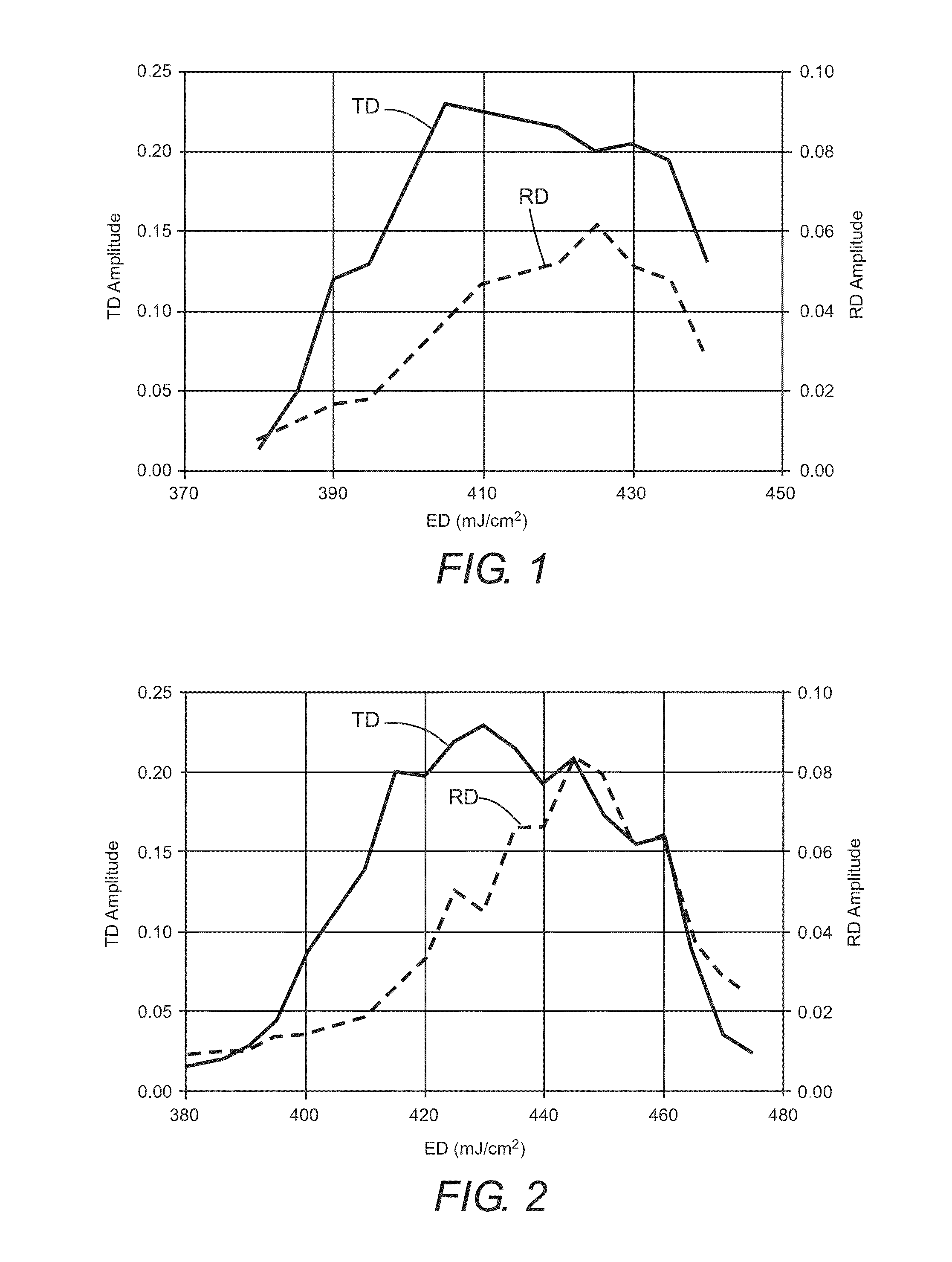
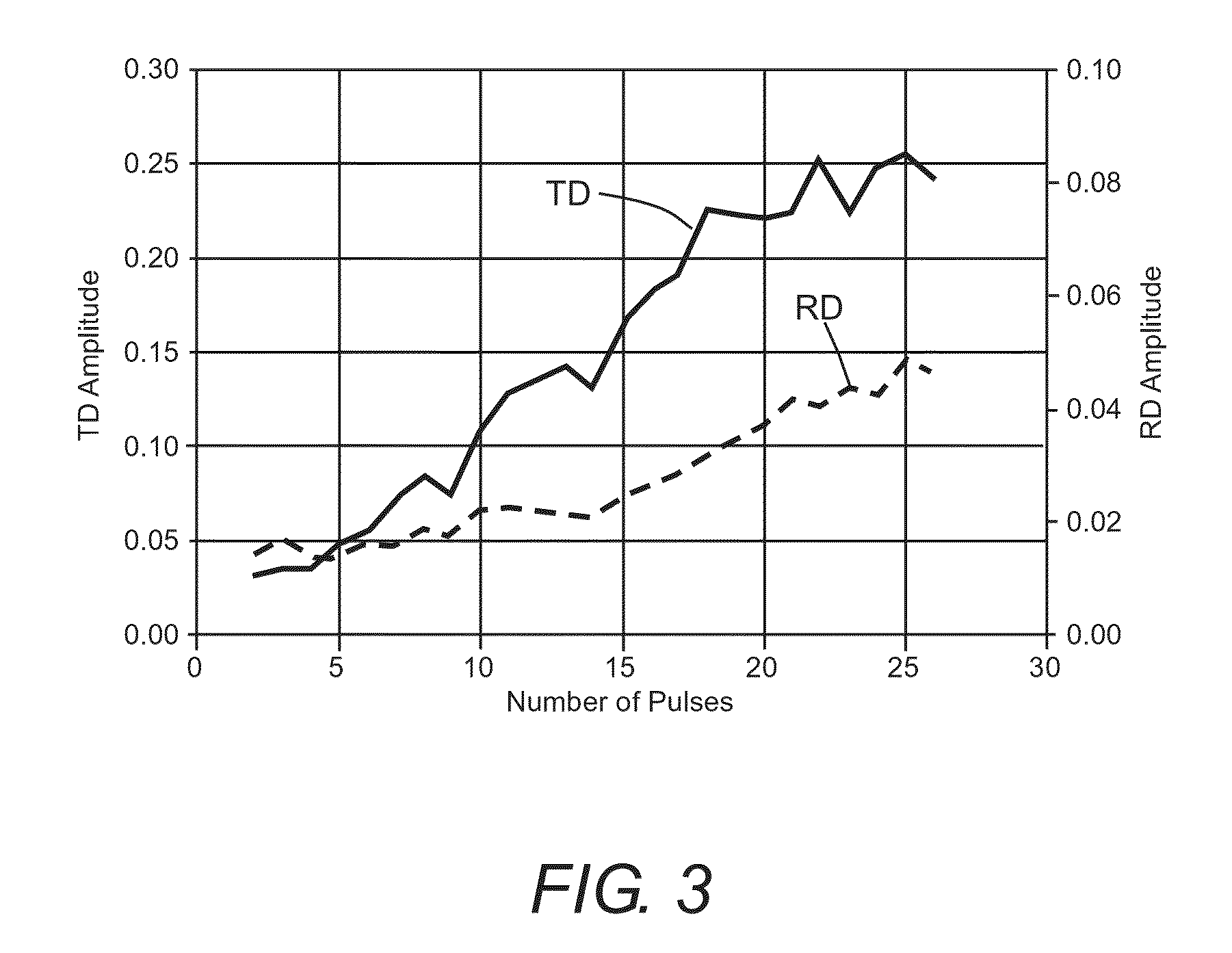
The present invention is about evaluating the progress of crystallization of a semiconductor layer using laser-radiation pulses. The laser-radiation pulses create regular surface features on the layer in two different directions. The evaluation method involves measuring the amplitudes of light that is scattered by these surface features. By measuring the energy density of the laser-radiation pulses, the evaluation method can provide a detailed analysis of the crystallization process and help improve the quality of the semiconductor layer.

Problems solved by technology

The process is a delicate one, and the error margin for OED can be a few percent or even as small as ±0.5%
In a manufacturing environment, the process of visual analysis and establishing if a change of process energy density is necessary typically takes between about one and one and one-half hours from when the crystallization was performed, with a corresponding adverse effect on production line throughput of acceptable panels.

Method used


Image

  • Monitoring method and apparatus for excimer laser annealing process
  • Monitoring method and apparatus for excimer laser annealing process
  • Monitoring method and apparatus for excimer laser annealing process

Examples


Embodiment Construction

[0021]ELA processing of thin Si films leads to formation of surface roughness: protrusions are formed as a result of the expansion of Si upon solidification; they are formed especially between three or more solidification fronts colliding during lateral growth. The protrusions are often not randomly located. Rather, they are aligned due to processes of ripple formation collectively referred to in the literature as laser-induced periodic surface structures (LIPSS). The ripples thus consist of series of well aligned protrusions. The ripple formation is only observed within an energy density window (range) in which partial melting of the film is achieved. Typically the ripple periodicity is on the order of the wavelength of the incident light, for example, around 290-340 nm for XeCl excimer lasers. Because of these small dimensions, ripples cannot or can at best hardly be resolved using conventional optical microscopy techniques.

[0022]What is typically observed in optical bright field ...


PUM

PropertyMeasurementUnit
Angleaaaaaaaaaa
Angleaaaaaaaaaa
Energyaaaaaaaaaa

Abstract

A method is disclosed evaluating a silicon layer crystallized by irradiation with pulses form an excimer-laser. The crystallization produces periodic features on the crystalized layer dependent on the number of and energy density in the pulses to which the layer has been exposed. An area of the layer is illuminated with light. A detector is arranged to detect light diffracted from the illuminated area and to determine from the detected diffracted light the energy density in the pulses to which the layer has been exposed.

Description

PRIORITY CLAIM[0001]This application claims priority of U.S. Provisional Application No. 61 / 663,435, filed Jun. 22, 2012, the complete disclosure of which is hereby incorporated herein by reference.TECHNICAL FIELD OF THE INVENTION[0002]The present invention relates in general to melting and recrystallization of thin silicon (Si) layers by pulsed laser irradiation. The method relates in particular to methods of evaluating the recrystallized layers.DISCUSSION OF BACKGROUND ART[0003]Silicon crystallization is a step that is often used in the manufacture of thin-film transistor (TFT) active-matrix LCDs, and organic LED (AMOLED) displays. The crystalline silicon forms a semiconductor base, in which electronic circuits of the display are formed by conventional lithographic processes. Commonly, crystallization is performed using a pulsed laser beam shaped in a long line having a uniform intensity profile along the length direction (long-axis), and also having a uniform or “top-hat” intensi...

Claims


Application Information

Patent Timeline
IPC IPC(8): G01N21/95H01L21/324C30B13/24
CPCG01N21/9501C30B13/24H01L21/324B23K26/083B23K26/355C30B13/28C30B29/06G01N21/4788G01N21/8422G01N2021/8461G01N2021/8477H01L21/02532H01L21/02587H01L21/02686H01L21/268H01L22/12B23K26/0622
Inventor VAN DER WILT, PAUL
Owner COHERENT LASERSYST
Learn More