Optical inspection method and optical inspection apparatus

Inactive Publication Date: 2013-12-12
HITACHI LTD
View PDF5 Cites 4 Cited by
  • Summary
  • Abstract
  • Description
  • Claims
  • Application Information

AI Technical Summary

Benefits of technology

The present invention provides a light convertor that improves defect detection by reducing the influence of quantum noise and accurately detecting the presence or absence of defects. This allows for better sensitivity and faster inspection times while maintaining accuracy.

Problems solved by technology

In this case, following the detection of the light by the detector, it is intrinsically impossible to suppress the influence of quantum noise.
In the past, however, no conversion was performed in order to suppress the influence of quantum noise on the interference with the reference light.
For this reason, when the quantity of light was small, it was impossible to obtain good defect detection performance.

Method used


Image

  • Optical inspection method and optical inspection apparatus
  • Optical inspection method and optical inspection apparatus
  • Optical inspection method and optical inspection apparatus

Examples


first embodiment

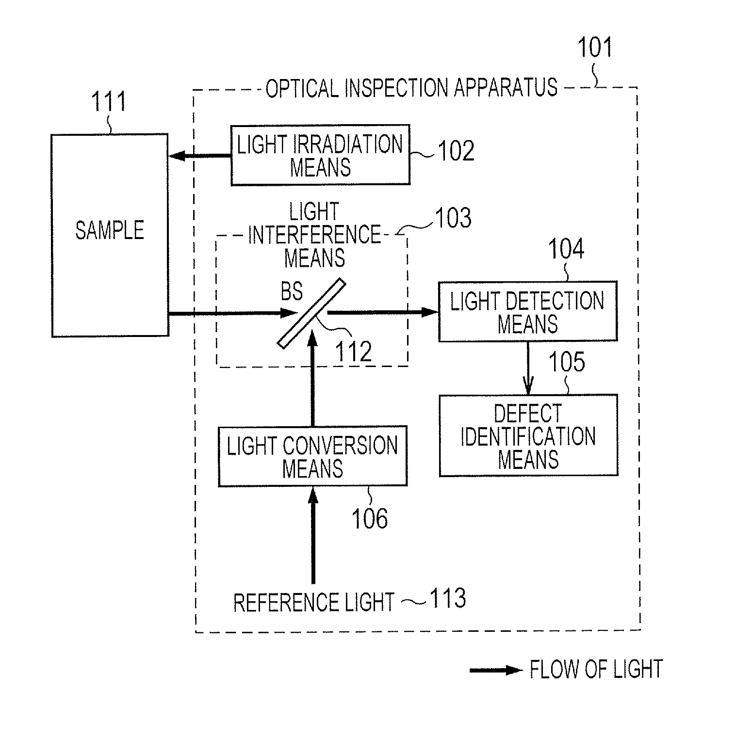
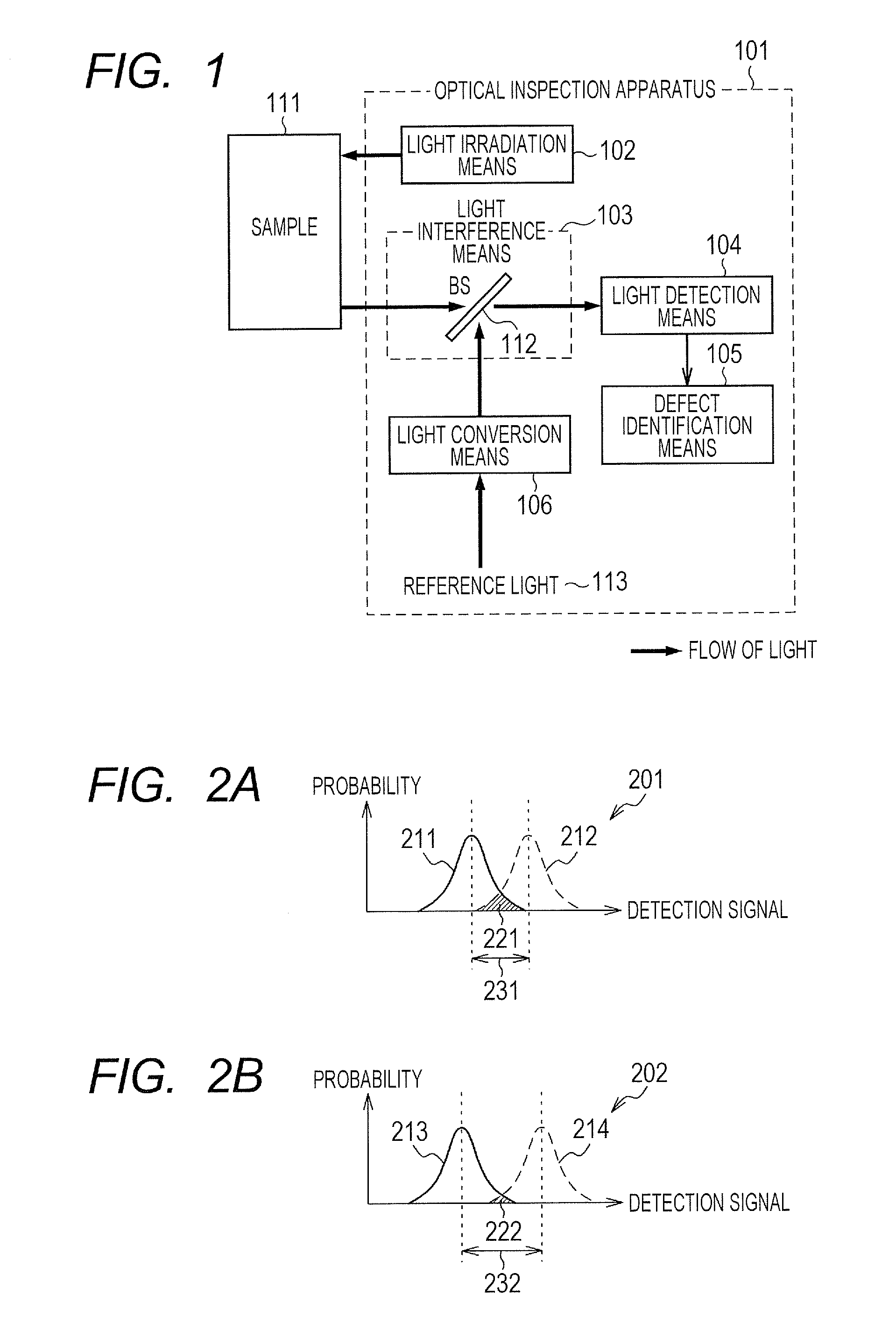
[0055]FIG. 1 shows a typical optical inspection apparatus 101 as the first embodiment that inspects a minute defect that may exist on the surface of a sample irradiated with light.

[0056]The optical inspection apparatus 101 is structured to include light irradiation means 102 for irradiating a sample 111 with light, light interference means 103 for causing the light scattered or reflected from the sample to interfere with reference light emitted by reference light source means 113, light detection means 104 for detecting the interfering light, and defect identification means 105 for identifying the presence or absence of a defect by processing a detection signal output from the light detection means 104 having detected the interfering light. The light with which the light irradiation means 102 irradiates the sample 111 is often focused onto the sample 111 so that the sample surface may be scanned with the focused light for enhancing spatial resolution. However, this is not limitative...

second embodiment

[0097]Explained below in reference to FIGS. 11A through 16 are examples formed by use of nonlinear conversion means as the light conversion means 106 in the structure shown in FIG. 1.

[0098]FIGS. 11A through 11D are illustrations each showing an example in which the light conversion means 106 shown in FIG. 1 is replaced with light conversion means that converts the state of target light, reference light, or light derived from interference between the target light and reference light through nonlinear conversion using a photonic crystal. Nonlinear conversion is a type of conversion whereby the electromagnetic field representing output light is not proportional to the electromagnetic field representative of input light. The photonic crystal is a structure in which materials of different refractive indexes are cyclically arrayed. As such, the structure is known to provide properties not available with conventional optical devices. In particular, using the photonic crystal permits fabric...

third embodiment

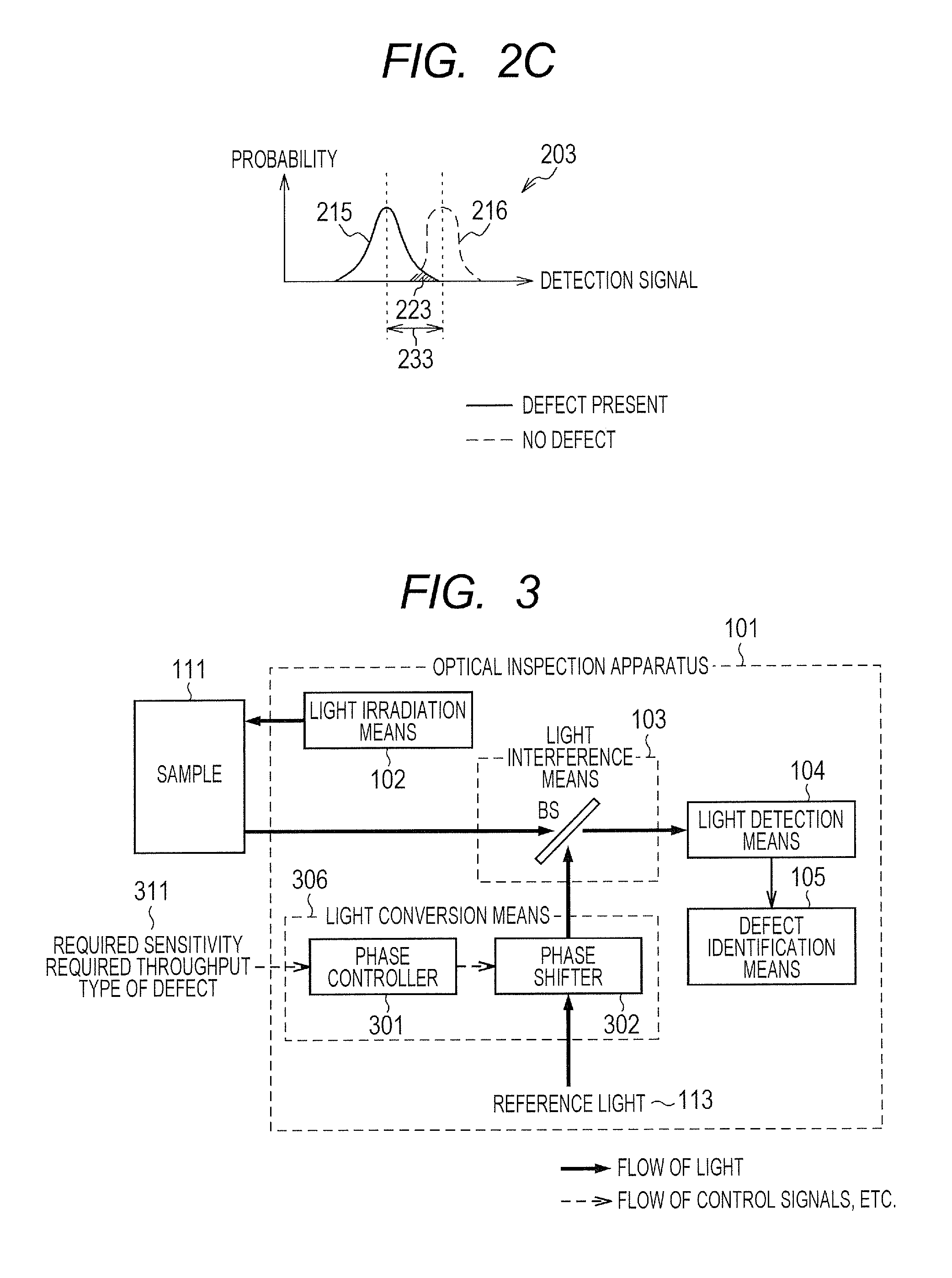
[0114]FIGS. 17A and 17B are illustrations showing structures of optical inspection apparatuses which include the light interference means 103 and light conversion means 103 or 306, among others, explained in conjunction with the first or the second embodiment and in which a sample is irradiated with light and the reflected light from the sample is received by the light interference means 103 and light conversion means 103 or 306.

[0115]FIG. 17A shows a structure of an inspection apparatus that irradiates a sample 1705 on a table 1721 with a light source 1701 from a perpendicular direction by epi-illumination for detection of a defect. Light 1706 emitted by the light source 1701 is focused by a lens 1703 onto the sample 1705 for epi-illumination of the sample 1705. Of the reflected light from the sample 1705, a light beam 1707 reflected in the direction of a lens 1704 is focused thereby for input to a receiver 1702. The receiver 1702 includes the light interference means (103), light ...


PUM


Abstract

An optical inspection apparatus is provided which suppresses the influence of quantum noise including: light irradiator which irradiates a sample with light; reference light emitter which emits reference light; light interference unit which generates interfering light through interference between transmitted light, scattered light, or reflected light from the sample irradiated with light by the light irradiator, and the reference light emitted by the reference light emitter; light detector which detects the interfering light generated by the light interference unit; defect identifier which identifies the presence or absence of a defect based on a detection signal obtained by the light detector detecting the interfering light; and light convertor which converts at least the state of the transmitted, scattered, or reflected light from the sample, the state of the reference light emitted by the reference light emitter, or the state of the interfering light generated by the light interference unit.

Description

BACKGROUND[0001]The present invention relates to an optical inspection method and an optical inspection apparatus for inspecting a minute defect on the surface of a sample by irradiating the sample with light and detecting reflected light therefrom.[0002]In the manufacturing lines of semiconductor substrates, thin film substrates and the like, optical inspection apparatuses are used extensively to inspect minute defects on the surface of samples so as to acquire a high product yield (e.g., JP-9 (1997)-304289-A (Patent Literature 1) and JP-2006-201179-A (Patent Literature 2)). Generally, the optical inspection apparatus irradiates the sample surface with a focused light beam of several tens of μm across, detects transmitted light, scattered light, or reflected light from any defect, and focuses the detected light for defect detection. Currently commercialized apparatuses can inspect defects of several tens of nm or more across.[0003]Meanwhile, with advances in fine processing technol...

Claims


Application Information

Patent Timeline
IPC IPC(8): G01N21/88
CPCG01N21/88G01N21/956G01N21/9501G01N2021/8835
Inventor NAKAHIRA, KENJIHONDA, TOSHIFUMINAKATA, TOSHIHIKO
Owner HITACHI LTD
Why Eureka
Try Eureka