Photorefractive devices having sol-gel buffer layers and methods of manufacturing

a photorefractive device and buffer layer technology, applied in the field of photorefractive devices and fabrication methods, can solve the problems of failure of photorefractive devices and increase the holding time of gratings, and achieve the effects of faster grating rise and decay time, higher electric breakdown strength, and larger single pulse grating signals

Inactive Publication Date: 2013-12-05
NITTO DENKO CORP
View PDF11 Cites 3 Cited by
  • Summary
  • Abstract
  • Description
  • Claims
  • Application Information

AI Technical Summary

Benefits of technology

[0017]It has been discovered that photorefractive devices produced using the materials and methods disclosed herein can achieve up to 30% and higher electric breakdown strength compared to similar devices that contain only one kind of polymer buffer layers with similar thicknesses. The addition of the sol-gel buffer layer, in combination with the polymer buffer layer, provides unexpectedly improved benefits. For example, it has also been discovered that the photorefractive devices produced using the materials and methods disclosed herein can achieve two to three times faster grating rising and decay times compared to devices containing only one kind of polymer buffer layer with similar thicknesses. Furthermore, it has also been discovered that the photorefractive devices produced using the materials and methods disclosed herein can achieve two to three times larger single pulse grating signals compared to devices containing only one kind of polymer buffer layer with similar thicknesses.

Problems solved by technology

While applying a high biased voltage may result in a better performance, the application of the high voltage in photorefractive material may also cause electrical breakdown which will lead to failure of the photorefractive device.
However, good electric breakdown protection typically requires relatively thicker polymer protection layers, which may result in an increase of the grating holding time.

Method used


Image

  • Photorefractive devices having sol-gel buffer layers and methods of manufacturing
  • Photorefractive devices having sol-gel buffer layers and methods of manufacturing
  • Photorefractive devices having sol-gel buffer layers and methods of manufacturing

Examples


example 1

Preparation of Photorefractive Devices

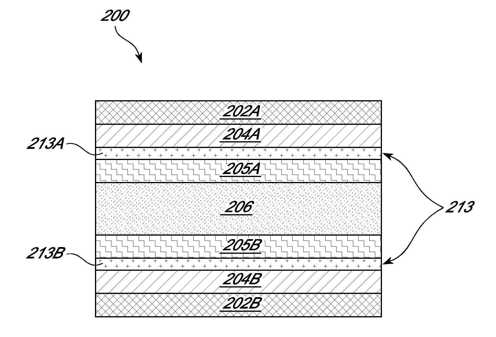
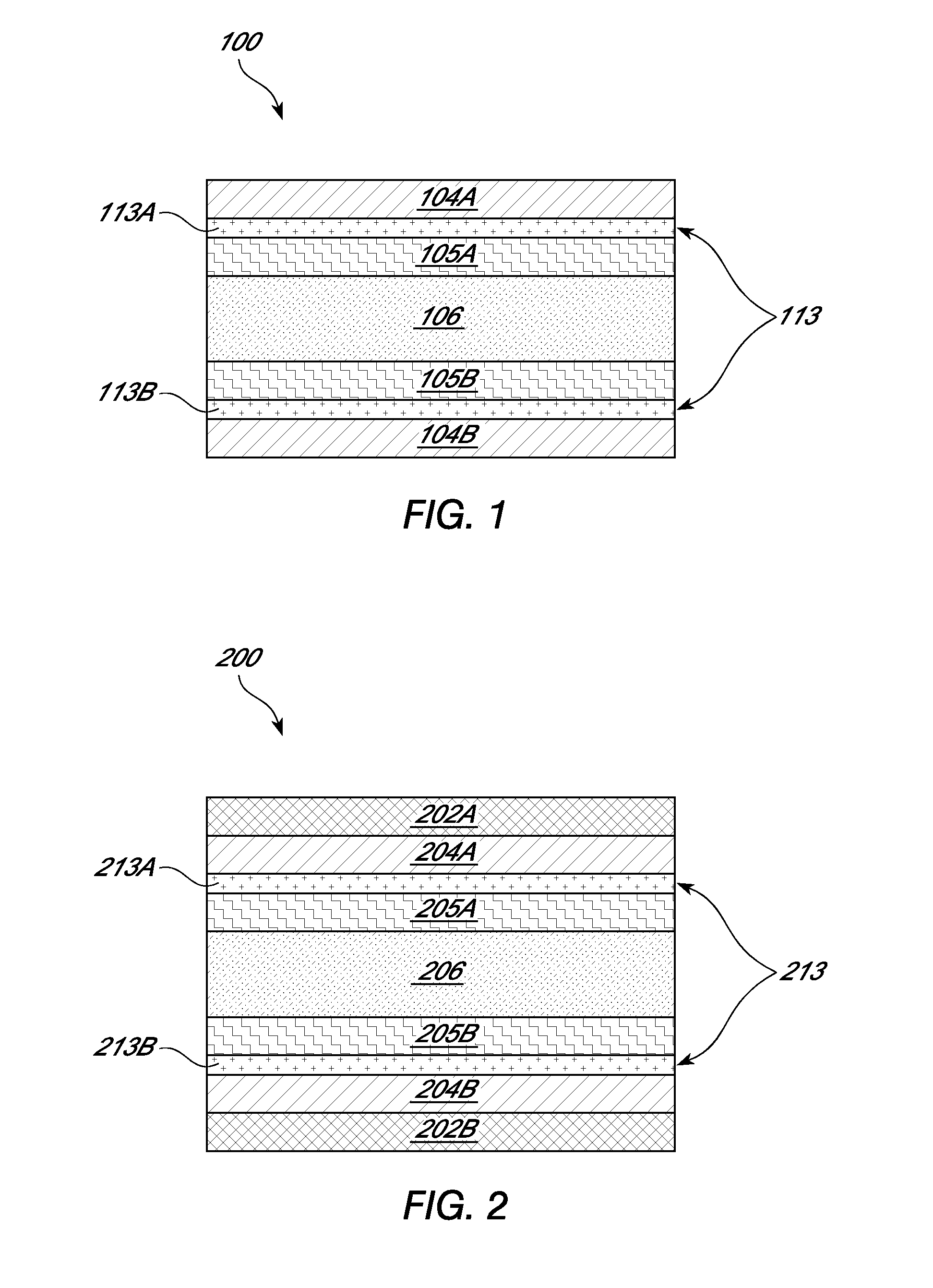
[0104]A photorefractive device was prepared having generally the same structure and components as shown in FIG. 2. From the outer layers to the inner layer were: two ITO-coated glass substrates (electrode and substrate), two sol-gel buffer layers, two polymer buffer layers, and a photorefractive layer. The photorefractive device was fabricated using the following steps:

[0105](i) Sol-gel solution: About 30 ml of MATMS was mixed with about 10 ml of absolute alcohol and stirred at about 60 degrees C. for about 10 minutes. Thereafter, about 2 ml of 0.2M HCl was added and stirred for about 4 hours at 60 degrees C. Then, about 3 ml of distilled water was added and stirred for about 2 hours at 60 degrees C. After cooling the solution down to room temperature, the solution was then mixed with about 17 ml of zirconium (IV) propoxide / MMA solution (about 4 ml MMA and about 13 ml zirconium (IV) propoxide 70% 1-propanol) and stirred at room temperature for a...


PUM

PropertyMeasurementUnit
dielectric constantaaaaaaaaaa
refractive indexaaaaaaaaaa
thicknessaaaaaaaaaa

Abstract

A photorefractive device (100) and methods of its manufacture are disclosed. The photorefractive device (100) comprises one or more transparent electrode layers (104), one or more sol-gel buffer layers (113), one or more polymer buffer layers (105), and a photorefractive layer (106). The one or more sol-gel buffer layer (113) is interposed between the one or more polymer buffer layer (105) and the one or more transparent electrode layer (104). When a bias voltage is applied to the device (100), the device (100) exhibits improvement in electric breakdown strength compared to a similar device without the one or more dielectric sol-gel buffer layers (113). The device (100) can operate at high bias levels with quick rising and decay times and shows higher grating performance under single nanosecond pulse recording conditions.

Description

CROSS-REFERENCE TO RELATED APPLICATIONS[0001]The present application claims priority under 35 U.S.C. §119(e) to U.S. Provisional Application No. 61 / 444,605 filed on Feb. 18, 2011, the disclosures of which is incorporated by reference herein in its entirety.STATEMENT REGARDING FEDERALLY SPONSORED R&D[0002]This invention was made with government support under FA8650-10-C-7034 awarded by the Office of the Director of National Intelligence (ODNI), Intelligence Advance Research Projects Activity (IARPA), through the Air Force Research Laboratory (AFRL). The government has certain rights in the invention.BACKGROUND OF THE INVENTION[0003]1. Field of the Invention[0004]The invention relates to photorefractive devices and fabrication methods for improving the performances of photorefractive devices using one or more sol-gel buffer layers. The implementation of one or more sol-gel buffer layers in the photorefractive devices improves properties, such as obtaining high electric breakdown stren...

Claims


Application Information

Patent Timeline
Patent Type & Authority Applications(United States)
IPC IPC(8): G02F1/29
CPCG02F1/293G02F1/0126G02F1/061G02F2202/13G02F2202/38G03H2001/026G03H2001/0264G03H2260/36G03H2260/54
Inventor WANG, PENGSIMAVORYAN, SERGEYLIN, WEIPINGHSIEH, WAN-YUNYAMAMOTO, MICHIHARU
Owner NITTO DENKO CORP
Why Eureka
Try Eureka