
3D Microfluidic Devices Based on Open-Through Thermoplastic Elastomer Membranes

a technology of thermoplastic elastomer and microfluidic device, which is applied in the direction of additive manufacturing apparatus, etc., can solve the problems of high cost and sophisticated tools, difficult to apply in point-of-care applications, and difficult control of accurate positioning and registration of spots, etc., and achieves high elasticity of tpe membranes, rapid, reliable and efficient patterning, and low cost

Active Publication Date: 2013-11-28
NAT RES COUNCIL OF CANADA
View PDF3 Cites 20 Cited by
  • Summary
  • Abstract
  • Description
  • Claims
  • Application Information

AI Technical Summary

Benefits of technology

The present invention provides open-through thermoplastic elastomer (TPE) membranes with micrometric open-through holes and other features that have a high aspect-ratio and can be formed without significant defects or deformations. The membranes have a high elasticity and low elastic modulus, which makes them suitable for use in microfluidic devices and other fields such as detection, biomarker discovery, and environmental and food safety. The membranes can be patterned using existing hot embossing processes and can be easily integrated into the fabrication of complex 3D microfluidic devices. The process is single step, does not require alignment of the mold and counter-plate, and can achieve open-through holes in TPE at low cost in a single or successive fabrication steps. The membranes have a high excess layer that separates systematically during demolding, which makes them compatible with low-cost photoresist-based molds and without the use of a receptor mold or sacrificial layer of polymer. The membranes can also be easily changed by elastic deformation of the TPE materials.

Problems solved by technology

However, microarrays still largely depend on detection techniques such as fluorescence labeling or surface plasmon resonance which are difficult to apply in point-of-care applications.
However, accurate positioning and registration of the spots are difficult to control and require costly and sophisticated tools.
Also, rapid and uncontrolled drying of the liquid deposited can lead to non-uniform spots and denaturing conditions, especially when the dimensions of the spots are decreased below about 80 μm.
On the other hand, simple microfluidic devices having a 2D network of channels are inherently limited to pattern continuous features and cannot be used to form an array of isolated spots, as it would be required, for example, to immobilize biological probes only on the sensing elements of a microfabricated biosensor array.
Although a device made from few layers of this TPE was briefly described, no method was unveiled to fabricate devices with a dense array of vias with TPE or to create microscopic open-through holes in such material.
This method cannot be used to create complex devices with 3D network of channels.
However, no 3D microfluidic devices were demonstrated or discussed.
Despite these recent developments, many challenges must still be solved before microfluidics can be accepted as a universal biological patterning tool.
Existing processes are typically very challenging, labor-intensive, and / or inherently serial.
Also, the properties of the materials used in such 3D devices are typically far from ideal.
As a consequence, the compatibility of the devices is often limited to only the most standard solvents and complicated and costly steps are required for the patterning and bonding of the multiple layers from which the devices are built.
These drawbacks have relegated 3D microfluidics to relatively simple academic prototyping and have largely dissuaded researchers and industries from further research on these methods.
The most critical issue arguably arises from the intrinsic need to use the microfluidic patterning devices only once to avoid cross-contamination issues.
Unfortunately, almost all previous designs of microfluidic patterning devices have relied on PDMS, which is not very amendable to low-cost mass-production.
It is also noteworthy that many of the 3D microfluidic designs proposed to date require the precise and difficult alignment of many elastomeric layers over large areas and the use of costly and lengthy post-processing procedures to punch the numerous access holes and cut the devices in final shape.
Although it has some very attractive properties such as high transparency, low hardness, elasticity, and relatively low cost, it also shows some serious drawbacks, which have precluded industry adoption of PDMS for mass production.
Firstly, as PDMS is a thermoset, it requires lengthy curing and degassing steps, which makes its use very unpractical for mass production.
This problem becomes critical for the fabrication of layered 3D devices, as many layers need to be degassed and cured independently for the fabrication of a single device.
The thermosetting properties of PDMS also prevent the use of simple techniques such as thermal bonding to assemble the final devices.
Another problem is the intrinsic porosity of PDMS and its relatively high gas permeability.
This problem is also strongly exacerbated in 3D layered devices due to the use of thin layers of PDMS (typically about 100 μm).
This process is not only inherently serial but is also very problematic due to the rather low mechanical strength of PDMS.
The PDMS membranes can thus break or deform very significantly during their manipulation, which makes alignment difficult or even impossible.
Finally, PDMS is not compatible with a large number of solvents and is thus relegated mostly to water-based chemistry.
Thus, although PDMS is very relevant for prototyping and academic demonstration of concepts, its use for the mass production of complex 3D layered devices is far from ideal.
They however have their own limitations.
The most important drawback comes from the rigid nature of these materials.
Contrary to elastomeric soft materials, hard materials do not allow reversible and conformal sealing on an arbitrary surface and do not offer the possibility of creating easily implementable valving schemes.
Fabrication of multi-layers 3D devices with hard materials is also typically more problematic than with PDMS.
The patterning of inorganic materials such as glass, silicon, metal, and ceramics cannot be performed with low cost rapid prototyping tools.
The production costs with these materials are thus generally too high to produce single-use complex 3D devices at reasonable price.
The patterning of hard thermoplastics is generally much easier than for hard inorganic materials, but it also presents some issues.
It is indeed very challenging to create microscopic open-through holes reliably in hard thermoplastics.
Under these conditions, it is not possible to use low cost photoresist-based molds (as typically used in PDMS molding), and costly metallic molds must be prepared.
The rigid nature of hard thermoplastics also makes demolding difficult or even impossible when high aspect ratio features are required.
Finally, it must be stressed that bonding is a difficult problem for most hard materials.
However, due to the high rigidity of these materials, microscopic defects, surfaces irregularities, or non ideal bonding conditions can easily result in partially bonded section and leaks.
As the probability of defect increases with the number of bonded layers, it can be very challenging to produce complex 3D devices in a reliable manner from hard materials.
Nevertheless, due to their rigid nature, hard materials are not compatible with applications requiring reversible and conformal sealing on arbitrary surfaces.
However, the lengthy and costly process of fabricating either a complex sacrificial 3D mold for each device or each 3D microfluidic device in a serial manner limits this technique to device design and early prototyping.
The printed 3D molds also typically have high roughness and a relatively low resolution (about 100 microns).
Finally, some types of features, such as long suspended channels, are difficult to create with this approach.
Although proof of concept for microfluidic immobilization of biological probes was obtained more than a decade ago, none of the microfluidic devices proposed to date can clearly combine all the characteristics necessary for widespread adoption of the technology.

Method used


Image

  • 3D Microfluidic Devices Based on Open-Through Thermoplastic Elastomer Membranes
  • 3D Microfluidic Devices Based on Open-Through Thermoplastic Elastomer Membranes
  • 3D Microfluidic Devices Based on Open-Through Thermoplastic Elastomer Membranes

Examples


example 1

Fabrication of TPE Membranes with Micrometric Open-Through Holes

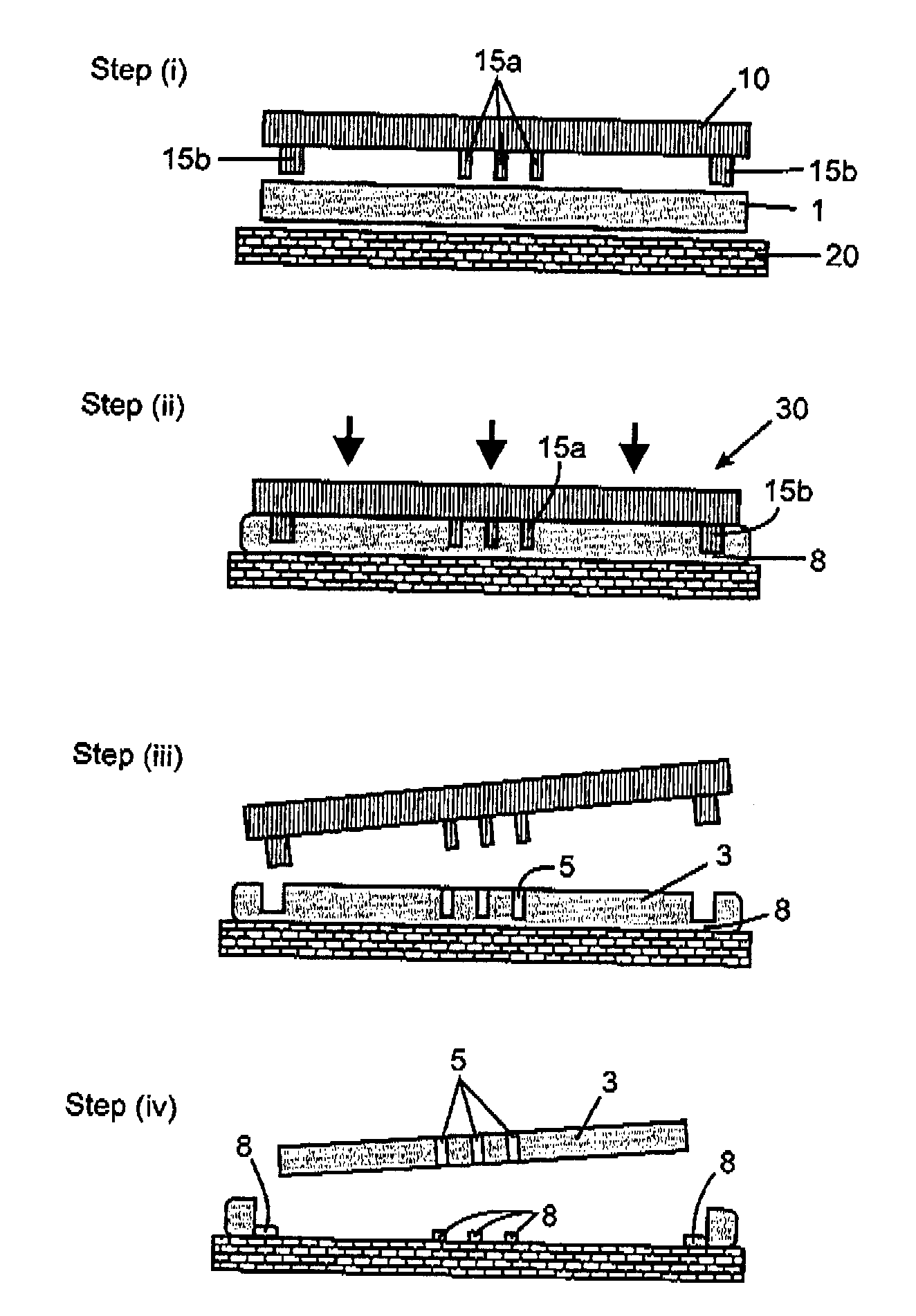
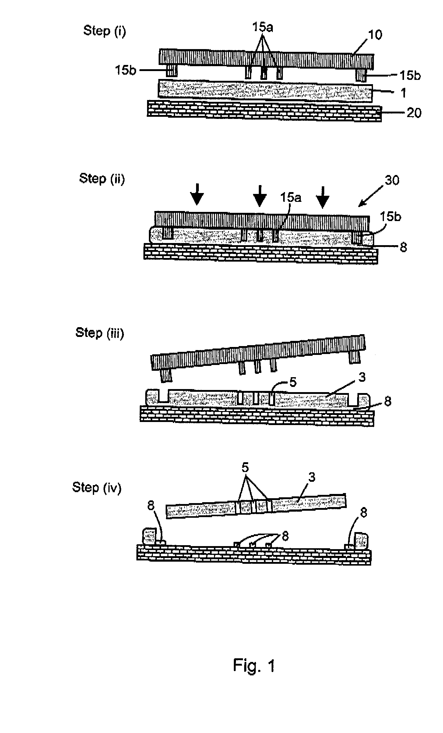
[0072]FIG. 1 illustrates schematically a process of the present invention for the fabrication of TPE membranes with open-through holes. As shown in FIG. 1 step (i), pre-extruded sheet 1 of TPE is first placed between mold 10 and flat counter plate 20. The TPE sheet has a thickness that almost matches or exceeds slightly that of highest features 15a,15b of the mold. The highest features include features 15a for producing open-through holes in the membrane and features 15b for cutting the membrane produced during hot embossing. As shown in FIG. 1 step (ii), assembly 30 is then heated to a temperature where the TPE is sufficiently softened and then pressed until the highest features of the mold nearly reach the counter plate, leaving only a submicron thick excess layer 8 of TPE between the highest features and the counter-plate. The thickness of excess layer 8 in FIG. 1 is exaggerated for clarity. As shown in FIG. 1 steps ...

example 2

Reducing Appearance of Defects in Open-Through TPE Membranes During Fabrication

[0077]Although the present process provides considerable benefits to the ease of patterning TPE, further improvement with respect to systematically improving the quality of the open-through TPE membranes would be beneficial. Stresses caused by the relatively high shrinkage (1-2%) of the TPE membrane during the cooling step can cause the appearance of defects when open-through holes are punched in the membranes. This is in contrast to hot embossing of TPE where open-through holes are not produced. FIG. 5A depicts a schematic diagram showing the patterning of TPE without open-through features. Stresses produced by shrinkage of TPE membrane 40 during cooling are relieved by vertical movement of counter-plate 41. In contrast, FIG. 5B depicts a schematic diagram showing the patterning of TPE with open-through features where counter-plate 45 cannot compensate for shrinkage of TPE membrane 44 during cooling and ...

example 3

Fabrication and Assembly of Open-Through TPE Membranes in a 3D Layered Microfluidic Device

[0081]A highly integrated 3D layered microfluidic spotter provides an example of a 3D microfluidic device based on open-through TPE membranes. The 3D micrometric patterning capability of the present process was used to produce a device that can bring liquid in contact only at some specific regions of a given substrate and that integrates a high density of inlet and outlets on a small footprint.

[0082]FIG. 6 is a schematic diagram summarizing an overall process for producing several 3D layered microfluidic spotters in one process. In the process, first open-through TPE membrane 100 is produced to contain elements that function as applicator heads for the spotter. Fabrication steps for the first membrane are shown on the left side of FIG. 6 (Steps 1-5). Second open-through TPE membrane 200 is produced to contain elements that function as spotting holes for the spotter and is fabricated in a simila...


PUM

PropertyMeasurementUnit
Tgaaaaaaaaaa
decomposition temperaturesaaaaaaaaaa
thickaaaaaaaaaa

Abstract

The invention provides a new process for patterning TPE membranes for use in the design and fabrication of 3D microfluidic devices. The process involves patterning a TPE material without permitting the highest features of the mold to come into contact with the counter-plate, whereby adhesion between the TPE and the mold or counter-plate during demolding results directly in removal of the excess layer from the TPE membrane to produce well formed micrometric-sized open-through holes in the TPE membrane. The process permits rapid, reliable and efficient patterning of densely packed and arbitrarily placed micrometric open-through holes and channels of high aspect-ratio and any shape or wall profile in thin TPE membranes.

Description

FIELD OF THE INVENTION[0001]The present invention is related to open-through thermoplastic elastomer (TPE) membranes, to methods of producing open-through TPE membranes and to three-dimensional microfluidic devices based on such membranes.BACKGROUND OF THE INVENTION[0002]The accurate deposition and patterning of biological probes on a solid support is of critical importance to numerous bioassays. For example, protein and DNA microarrays, which offer the interesting possibility to study concurrently the interaction between a target sample and a large number of different biological probes, have become key components of drug discovery, clinical diagnostics, and gene sequencing. However, microarrays still largely depend on detection techniques such as fluorescence labeling or surface plasmon resonance which are difficult to apply in point-of-care applications. Recently, new detection techniques involving integrated sensors with microfabricated biosensing elements have emerged, including...

Claims


Application Information

Patent Timeline
Patent Type & Authority Applications(United States)
IPC IPC(8): B29C51/00
CPCB29C51/00B29C43/021B29C43/04B33Y80/00B29C33/42B29C33/424B29C43/32
Inventor BRASSARD, DANIELROY, EMMANUELLI, KEBINVERES, TEODOR
Owner NAT RES COUNCIL OF CANADA
Learn More