Corrugated interfaces for multilayered interconnects

a multi-layered interconnect and corrugated technology, applied in the direction of printed element electric connection formation, insulation bodies, transportation and packaging, etc., can solve the problems of mechanical failure, adhesion failure, fracturing of one or more layers, etc., to increase the crack front tortuousity, increase the interlayer adhesion, and enhance the cracking/fracture resistance

Active Publication Date: 2013-10-17
TAIWAN SEMICON MFG CO LTD
View PDF5 Cites 0 Cited by
  • Summary
  • Abstract
  • Description
  • Claims
  • Application Information

AI Technical Summary

Benefits of technology

The patent text describes a new technology for making electronic devices using nanotechnology. The technology involves creating corrugated interfaces between layers of materials in an interconnect stack. The corrugations are formed in a controlled and reproducible way, and the device structure has improved performance and reliability. The text describes several methods for creating the corrugated interfaces, including using self-assembled patterns and adhesion promoters. Overall, the technology can be used to make more efficient and reliable electronic devices.

Problems solved by technology

With the advent of mechanically fragile low k and ultra low k dielectric currently being used or explored in these advanced applications, the issues of maintaining adequate interfacial adhesion as well as overall fracture toughness of the multilayer stack is becoming more important.
As shown, an interface 18 formed between the first and second dielectric film is substantially smooth, which can result in mechanical failure during fabrication of the device in which additional layers are added and patterns are formed thereon.
For example, adhesion failure and fracturing of one or more the layers can occur.
However, the topography provided by these treatments is generally random.
Moreover, the morphology in the lateral and vertical directions is difficult to control and reproduce.
The various known surface treatments such as those noted above can also lead to undesirable chemical modification of the substrate depending on the plasma gases employed.
For example, it is generally difficult with these processes to localize the chemical modification caused by plasma exposure of the substrate to the top surface (the interface) only.
In the case of low k dielectric films of interest for chip applications, the interconnect electrical characteristics (e.g., dielectric constant (k) and breakdown fields) can be significantly and undesirably degraded as a result of the plasma exposures.
Although the plasma treatment renders the organosilicate surface more hydrophilic and wettable, significant damage occurs throughout the depth of the organosilicate low k dilectric making this type of process unsuitable.
Damage manifests itself in the form of a higher dielectric constant (higher k) and lowers the breakdown strength of the dielectric.
Thus, the use of the above noted chemical means to enhance adhesion and fracture toughness in these structures is limited in practicality.
However, the use of mechanical profiling tools is generally impractical for use with interconnecting structures with thin dielectric layers because of the fragility of the microelectronic components and substrates, many or which are processed on fragile silicon wafers and comprise thin dielectric and metal films.
Thus, it is clear that suitable methods to achieve well controlled, non-damaging, reproducible, nanoscale corrugations in substrates and thin film coatings of interest in microelectronics is desirable and is not readily achieved by methods known in the current state of art.

Method used


Image

  • Corrugated interfaces for multilayered interconnects
  • Corrugated interfaces for multilayered interconnects
  • Corrugated interfaces for multilayered interconnects

Examples


Embodiment Construction

[0030]Self assembled films that laterally phase separate into regions with distinct compositions throughout the film are ideally suited as corrugation templates as the length scale in which the phase separation occurs can be in the range of approximately 5 to 100 nm. There are numerous examples of self assembled films that may be utilized for these purposes and they include a polymer mixture, a block copolymer, a mixture of homopolymer and block copolymer, a mixture of different block copolymers, a mixture of homopolymer and nanoparticles, a mixture of block copolymer and nanoparticles, sol-gel system containing surfactants, or any combination thereof. The invention is not intended to be limited to any particular type of self assembled film. By way of example, the polymers can contain block structures that contain spatially separated hydrophilic and hydrophobic blocks, i.e., amphiphilic polymers.

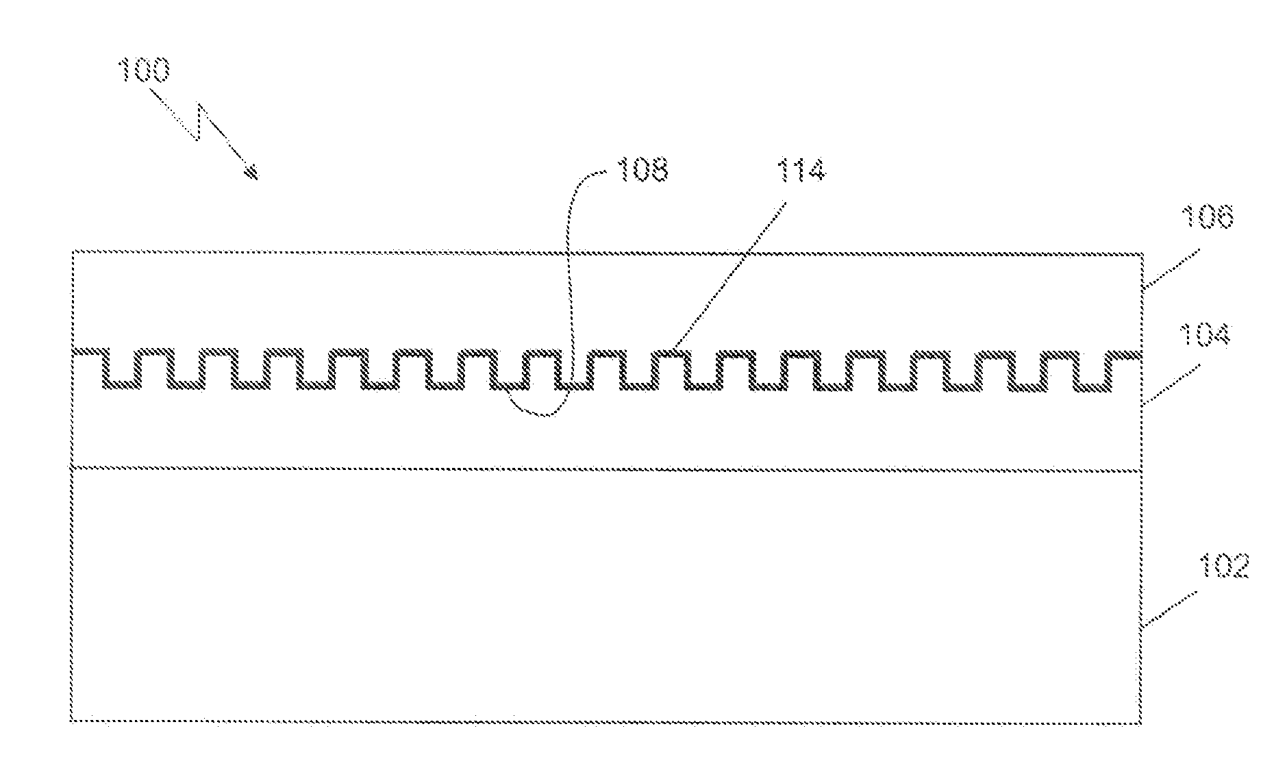
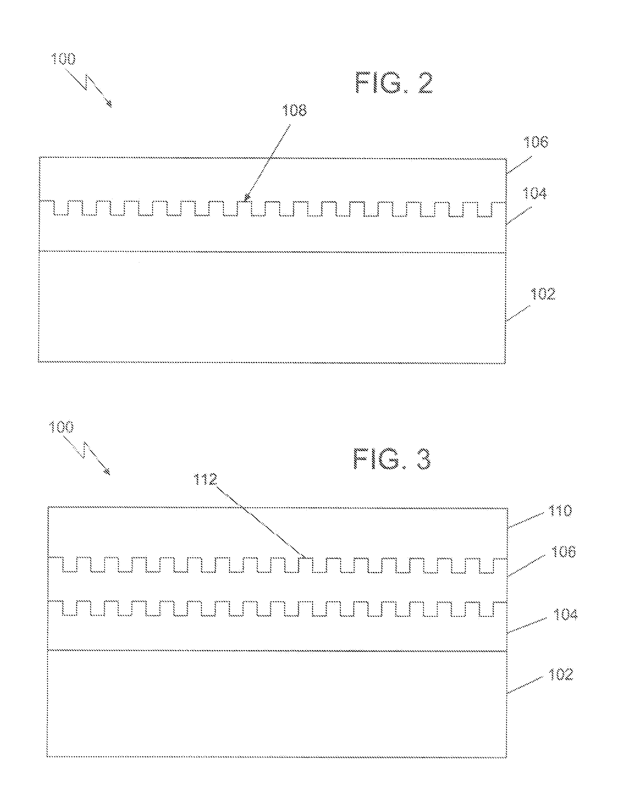
[0031]Referring now to FIG. 2, there is shown device 100 that includes controlled, nanom...


PUM

PropertyMeasurementUnit
diameteraaaaaaaaaa
diameteraaaaaaaaaa
wavelengthaaaaaaaaaa

Abstract

Dielectric composite structures comprising interfaces possessing nanometer scale corrugated interfaces in interconnect stack provide enhances adhesion strength and interfacial fracture toughness. Composite structures further comprising corrugated adhesion promoter layers to further increase intrinsic interfacial adhesion are also described. Methods to form the nanometer scale corrugated interfaces for enabling these structures using self assembling polymer systems and pattern transfer process are also described.

Description

CROSS-REFERENCE TO RELATED APPLICATION[0001]This application is a DIVISIONAL application of U.S. patent application Ser. No. 11 / 836,253, filed Aug. 9, 2007, the disclosure of which is also incorporated herein by reference in its entirety.FIELD OF THE INVENTION[0002]This invention relates to interconnect structures and more particularly to multi-layered interconnect structures wherein an interface between the layers includes a corrugated structure. The corrugated structure provides improved adhesion and fracture toughness, among others.DESCRIPTION OF BACKGROUND[0003]Advanced microelectronic interconnects can include multiple stacked layers of dielectric films. Due to the large number of interfaces between dielectric layers, interfacial adhesion is critical to ensure a reliable and robust structure that can survive the various fabrication processes and conditions used to fabricate the desired device. With the advent of mechanically fragile low k and ultra low k dielectric currently be...

Claims


Application Information

Patent Timeline
Patent Type & Authority Applications(United States)
IPC IPC(8): H01B17/66
CPCH01B17/66H01L21/0337H01L21/31144H01L21/76822H01L23/53295H01L2924/0002Y10T428/24537Y10T428/24612Y10T156/1039Y10T428/24529Y10T428/24711Y10T428/24521Y10T156/1082H01L2924/00H05K3/40
Inventor CLEVENGER, LAWRENCE A.DALTON, TIMOTHY J.HUANG, ELBERT E.PURUSHOTHAMAN, SAMPATHRADENS, CARL J.
Owner TAIWAN SEMICON MFG CO LTD
Why Eureka
Try Eureka