Photovoltaic junction for a solar cell

Active Publication Date: 2013-10-17
LUMENTUM OPERATIONS LLC
View PDF5 Cites 7 Cited by
  • Summary
  • Abstract
  • Description
  • Claims
  • Application Information

AI Technical Summary

Benefits of technology

The present invention relates to a photovoltaic junction structure that includes quantum wells with opposite stress types, which reduces the maximum stress difference between the wells and barriers. This is important for achieving extensions to longer wavelengths of the absorption edge of a photovoltaic junction. The use of two types of wells with opposite stress types helps to contribute to the shift to longer wavelengths of the absorption edge, and this effect is increased with increasing nitrogen concentration in the wells. The invention also includes additional doped semiconductor regions with either a higher doping or a higher bandgap, or both, to improve photocurrent collection efficiency. A mirror can also be included to improve photon absorption. The lattice constant refers to the spacing between the atoms in a material, and the term refers to the spacing that the material would naturally adopt without being influenced by adjacent materials with different lattice constants or actual lattice sizes.

Problems solved by technology

In some epitaxial growth conditions, nitrogen may tend to enhance indium segregation effects, leading to poor material quality in layers containing indium, and therefore reduced efficiency of the photovoltaic junction and solar cell.

Method used


Image

  • Photovoltaic junction for a solar cell
  • Photovoltaic junction for a solar cell
  • Photovoltaic junction for a solar cell

Examples


Embodiment Construction

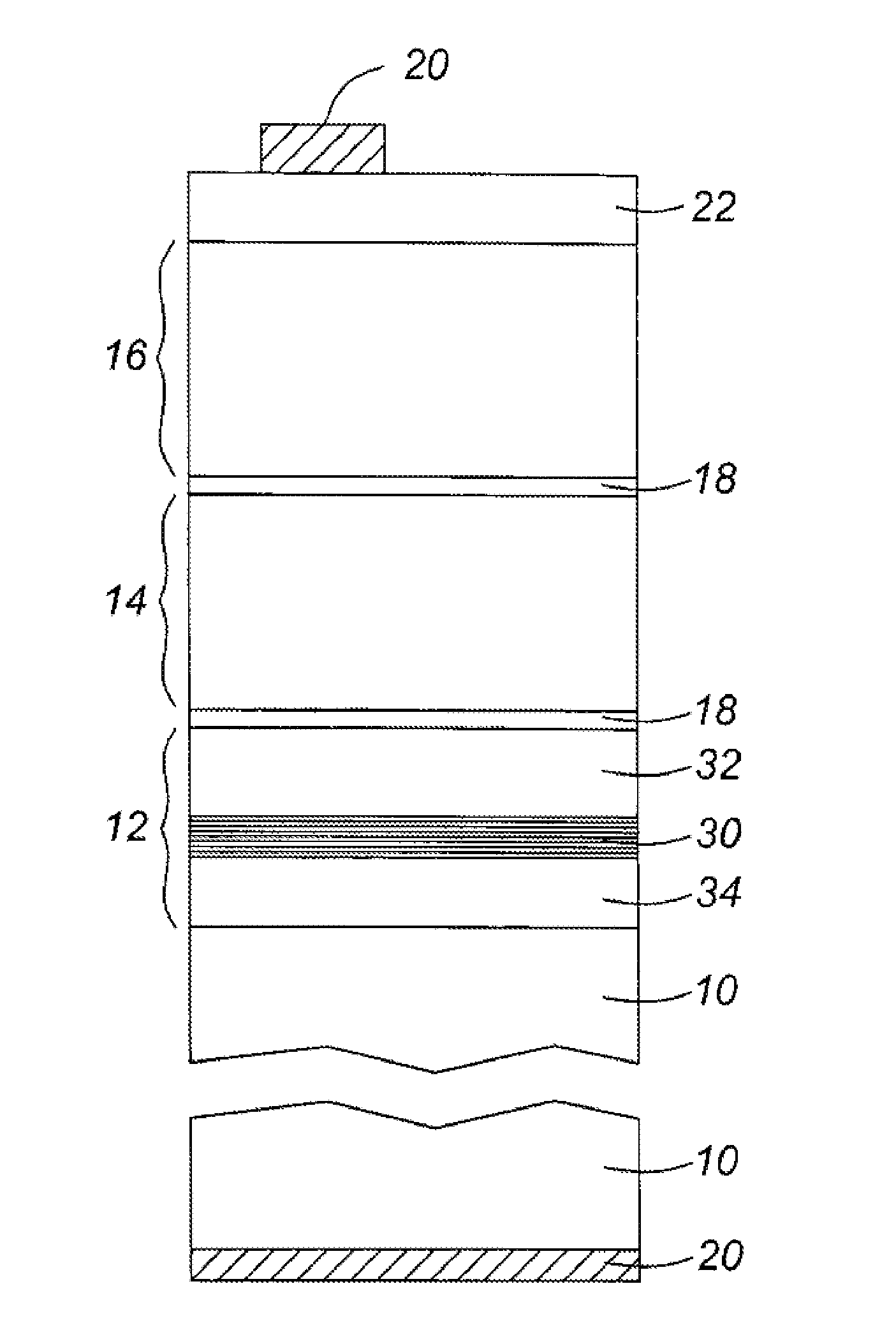
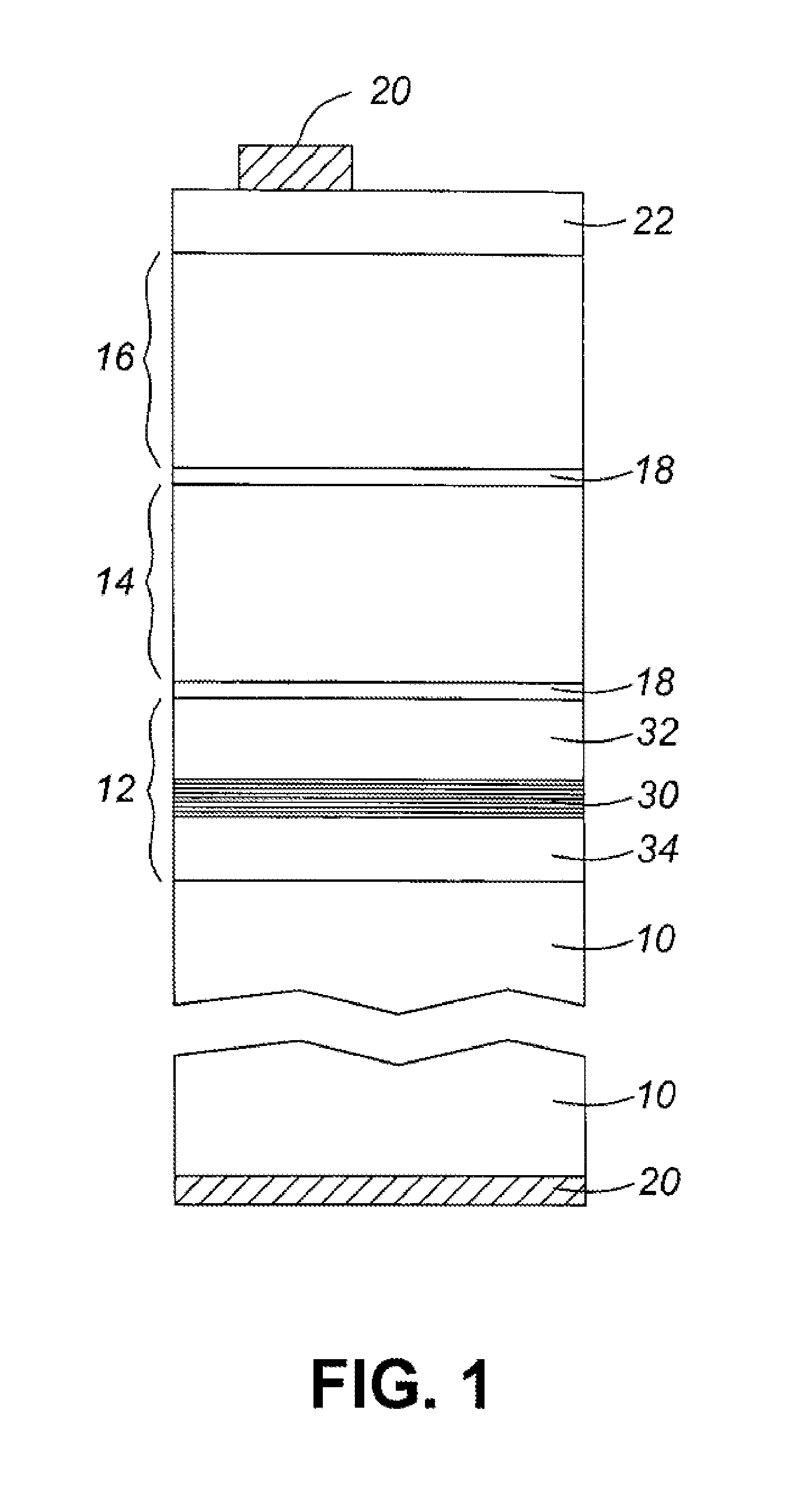
[0052]Referring now to FIG. 1, epitaxially grown layers of a solar cell according to a first embodiment of the invention are shown schematically in cross section. Not all layers are necessarily shown in the figure, and the layer thicknesses are not intended to be to scale. Broadly, the cell comprises a substrate 10 on which are formed one or more photovoltaic junctions. In this example, three photovoltaic junctions 12, 14, 16 are shown, but any suitable number may be used as required. The photovoltaic junctions are coupled using tunnel junctions 18, so that a common photocurrent passes through all of the junctions, for collection using electrodes 20 typically disposed beneath the substrate 10 to and on top of a window layer 22 overlying the uppermost photovoltaic junction 16. The photovoltaic junctions and other semiconductor layer structures are formed on the substrate using an epitaxial process such as chemical vapour deposition, to form a monolithic structure.

[0053]The substrate ...


PUM


Abstract

A photovoltaic junction for a solar cell is provided. The photovoltaic junction has an intrinsic region comprising a multiple quantum well stack formed from a series of quantum wells separated by barriers, in which the tensile stress in some of the quantum wells is partly or completely balanced by compressive stress in the others of the quantum wells. The overall elastostatic equilibrium of the multiple quantum well stack may be ensured by engineering the structural and optical properties of the quantum wells only, with the barriers having the same lattice constant as the materials used in the oppositely doped semiconductor regions of the junction, or equivalently as the actual lattice size of the junction or intrinsic region, or the bulk or effective lattice size of the substrate. Alternatively, the barriers may contribute to the stress balance.

Description

[0001]The present invention relates to a photovoltaic junction, for example for use in a solar cell, and in particular, to such a photovoltaic junction in which the intrinsic region contains a plurality of quantum wells formed of one or more materials having a lattice constant different to the actual lattice size of the junction.[0002]In particular, but not exclusively, the invention may be used in III-V semiconductor based concentrator solar cells, for example in such cells having multiple photovoltaic junctions grown monolithically in tandem based on a GaAs, SiGe or Ge substrate or lattice size.INTRODUCTION[0003]A photovoltaic cell usually comprises two or more layers of semiconductor material from which charge carriers are liberated by incident light, such as sunlight. One or more semiconductor junctions between the layers operate to separate the liberated charge carriers which then move to electrodes thereby providing electrical power.[0004]A photovoltaic junction for a solar ce...

Claims


Application Information

Patent Timeline
IPC IPC(8): H01L31/0352H01L31/18
CPCH01L31/035236H01L31/18B82Y20/00H01L31/03048H01L31/075H01L31/1848Y02E10/544Y02E10/548H01L27/142H01L31/0304
Inventor MAZZER, MASSIMOTIBBITS, THOMASBROWNE, BEN
Owner LUMENTUM OPERATIONS LLC
Why Eureka
Try Eureka