Eureka AIR delivers breakthrough ideas for toughest innovation challenges, trusted by R&D personnel around the world.

Nano-complex thermoelectric material, and thermoelectric module and thermoelectric apparatus including the same

a thermoelectric material and thermoelectric technology, applied in the manufacture/treatment of thermoelectric devices, non-metal conductors, conductors, etc., can solve the problems of increasing the demand for thermoelectric materials in the precise temperature control system of dna applications where conventional refrigerant gas compression system is ineffective, and the use of passive cooling system is inefficient, so as to achieve low thermal conductivity and high seebeck coefficient and electrical conductivity

Active Publication Date: 2013-10-17
SAMSUNG ELECTRONICS CO LTD
View PDF3 Cites 20 Cited by
  • Summary
  • Abstract
  • Description
  • Claims
  • Application Information

AI Technical Summary

Benefits of technology

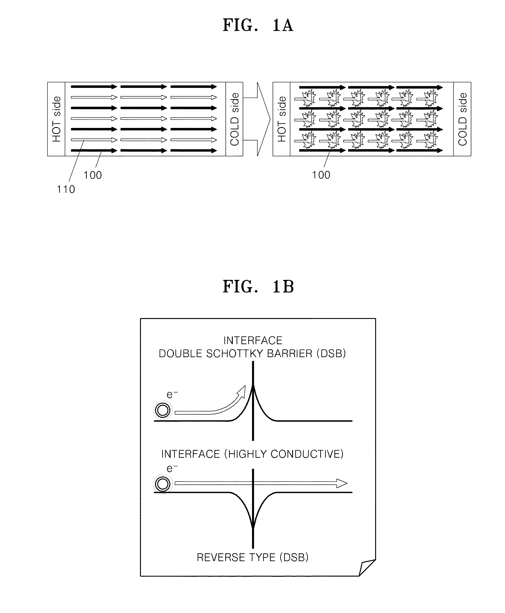
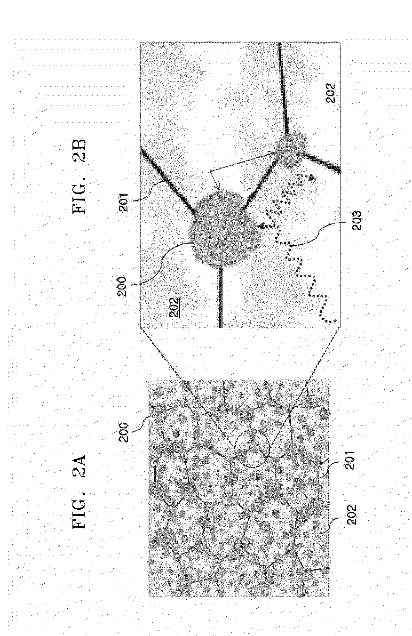
The patent describes a new type of thermoelectric material that has high electrical conductivity, low thermal conductivity, and a high Seebeck coefficient. This material can be used in thermoelectric modules and apparatuses to efficiently absorb and convert heat. The method of manufacturing involves creating metal nanoparticles and adding them to a thermoelectric matrix powder. The resulting material can be dried and heat treated for better performance.

Problems solved by technology

Currently, thermoelectric materials are used in active cooling systems of semiconductor equipment and electronic devices for which use of a passive cooling system is inefficient.
In addition, demands for thermoelectric materials in areas such as precise temperature control systems in DNA applications where conventional refrigerant gas compression systems are ineffective have increased.

Method used


Image

  • Nano-complex thermoelectric material, and thermoelectric module and thermoelectric apparatus including the same
  • Nano-complex thermoelectric material, and thermoelectric module and thermoelectric apparatus including the same
  • Nano-complex thermoelectric material, and thermoelectric module and thermoelectric apparatus including the same

Examples


example 1

Preparation of a Bi0.5Sb1.5Te3 Powder

[0105]A Bi—Te alloy was prepared as a thermoelectric semiconductor matrix (a starting material). In order to prepare the Bi—Te alloy, Bi, Sb, and Te, which are raw materials, were weighed at a molar ratio of 0.5:1.5:3, put in a quartz tube, sealed in a vacuum under 10−4 torr, melted at a temperature of 650° C. or higher, and rapidly cooled to prepare an alloy ingot having a composition of Bi0.5Sb1.5Te3. The alloy ingot was ground into a powder having a particle size of several millimeters and then ground again using a high-energy milling method. The Bi0.5Sb1.5Te3 powder was sorted into a powder having a size less than or equal to several tens of micrometers using a mechanical sieve (325 mesh) to obtain an initial powder. The p-type alloy powder having the composition Bi0.5Sb1.5Te3 was used as a thermoelectric matrix.

Preparation of a Bi0.5Sb1.5Te3 Nano-Complex Thermoelectric Material Powder Incorporated with 0.2 wt % of Si

[0106]0.05192 grams (g) o...

example 2

[0108]A nano-complex thermoelectric material was prepared in the same manner as in Example 1, except that 0.01480 g of terbium (III) acetate hydrate was used instead of 0.05192 g of tetraethoxysaline.

example 3

[0109]A nano-complex thermoelectric material was prepared in the same manner as in Example 1, except that 0.01488 g of gadolinium (III) acetate hydrate was used instead of tetraethoxysaline.


PUM

PropertyMeasurementUnit
diameteraaaaaaaaaa
thermoelectricaaaaaaaaaa
work functionaaaaaaaaaa

Abstract

A thermoelectric material including: a thermoelectric matrix; and a plurality of metal nanoparticles disposed in the thermoelectric matrix, wherein a difference between a work function of thermoelectric matrix and a work function of a metal particle of the metal nanoparticles is about −1.0 electron volt to about 1.0 electron volt.

Description

[0001]This application claims priority to and the benefit of Korean Patent Application No. 10-2012-0004907, filed on Jan. 16, 2012, and all the benefits accruing therefrom under 35 U.S.C. §119, the content of which is incorporated herein in its entirety by reference.BACKGROUND[0002]1. Field[0003]The present disclosure relates to a nano-complex thermoelectric material, and a thermoelectric module and a thermoelectric apparatus including the nano-complex thermoelectric material, and more particularly, to a nano-complex thermoelectric material, and a thermoelectric module and a thermoelectric apparatus including the nano-complex thermoelectric material having a high Seebeck coefficient, high electrical conductivity, and low thermal conductivity.[0004]2. Description of the Related Art[0005]The thermoelectric effect is a reversible, direct energy conversion from heat to electricity and vice versa, which occurs when electrons and holes move in a material.[0006]Examples of the thermoelectr...

Claims


Application Information

Patent Timeline
Patent Type & Authority Applications(United States)
IPC IPC(8): H01L35/16H10N10/85H10N10/852H10N10/01H10N10/857
CPCH01L35/16H10N10/857H10N10/852H10N10/85H10N10/01
Inventor HWANG, SUNG-WOOLEE, KYU-HYOUNGKIM, SANG-ILAHN, KYUNG-HAN
Owner SAMSUNG ELECTRONICS CO LTD
Why Eureka
Eureka Blog
Learn More