
Light-emitting panel and head up display including the same

a technology of light-emitting panels and head-up displays, applied in static indicating devices, lighting and heating apparatus, instruments, etc., can solve problems such as characteristic deterioration of light-emitting devices, and achieve the effect of effective release of heat and prevention of characteristic deterioration

Inactive Publication Date: 2013-08-01
OKI DATA CORP
View PDF13 Cites 14 Cited by
  • Summary
  • Abstract
  • Description
  • Claims
  • Application Information

AI Technical Summary

Benefits of technology

The patent text describes a way to improve the efficiency of a light-emitting device by using a microlens array to narrow the angle of the light distribution. The invention also focuses on effectively releasing heat that is generated by external light in thin-film semiconductor devices. This prevents temperature-related deterioration and ensures the devices perform optimally.

Problems solved by technology

Such a local temperature rise causes the problem of light-emitting device characteristic deterioration, such as a brightness deterioration.

Method used


Image

  • Light-emitting panel and head up display including the same
  • Light-emitting panel and head up display including the same
  • Light-emitting panel and head up display including the same

Examples


first embodiment

[0032]A description is provided for the First Embodiment of the invention with reference to FIGS. 1 to 8.

Configuration

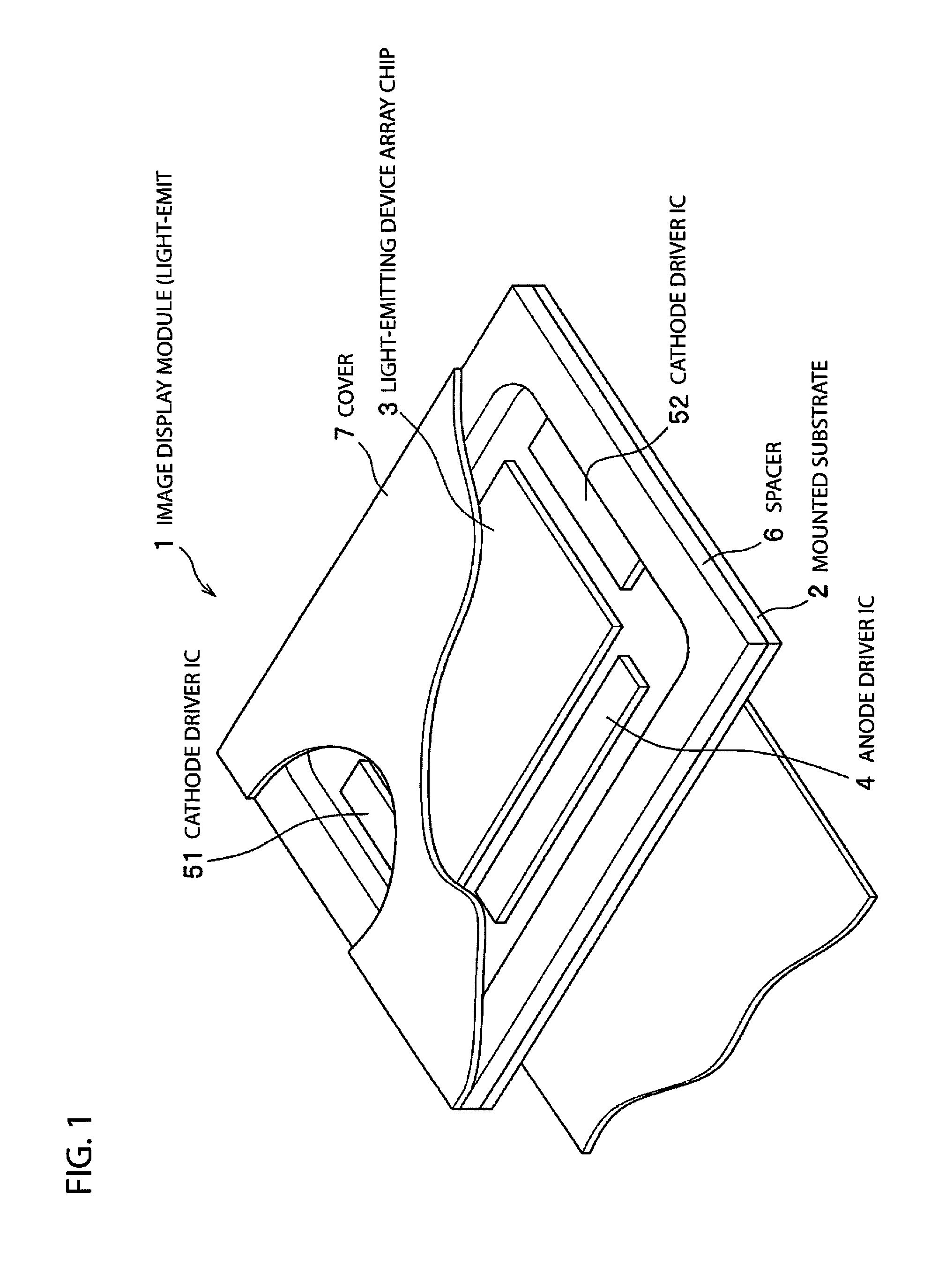
[0033]FIG. 1 is an outline perspective diagram for explaining the entire image display module 1 in the First Embodiment of the invention. Image display module 1 includes mounted substrate 2 for mounting a semiconductor chip (for example, a chip on board: COB). Mounted substrate 2 is formed with a silicon substrate, a glass epoxy substrate, an alumina substrate, an aluminum nitride (AlN) substrate, a metal substrate, a metal core substrate or the like and includes an unillustrated wiring pattern and the like formed in a surface thereof.

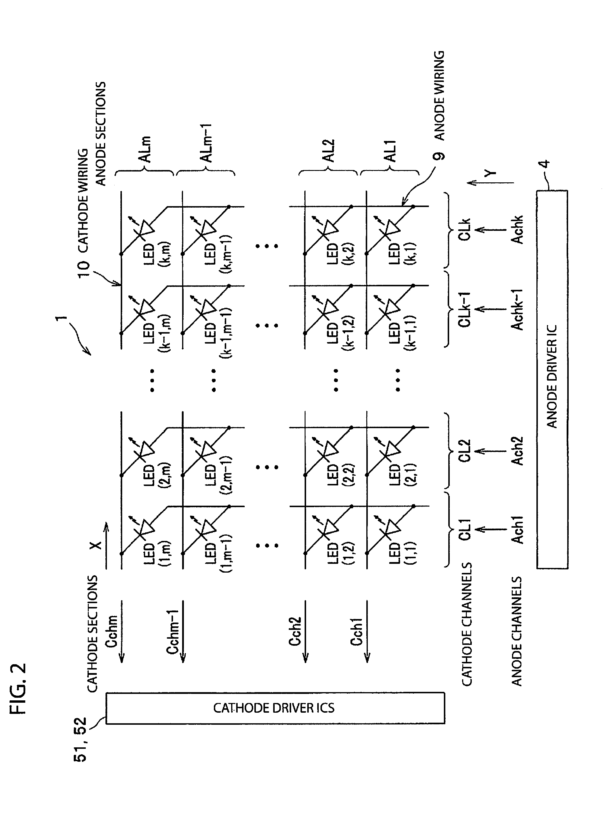
[0034]Light-emitting device array chip 3 formed by using thin-film semiconductor light-emitting devices (for example, LEDs), anode driver integrated circuit 4 (hereinafter, referred to as “anode driver IC 4”) which is a driving circuit for driving light-emitting device array chip 3, and cathode driver ICs 51, 52 are fixed on a surface o...

second embodiment

Configuration

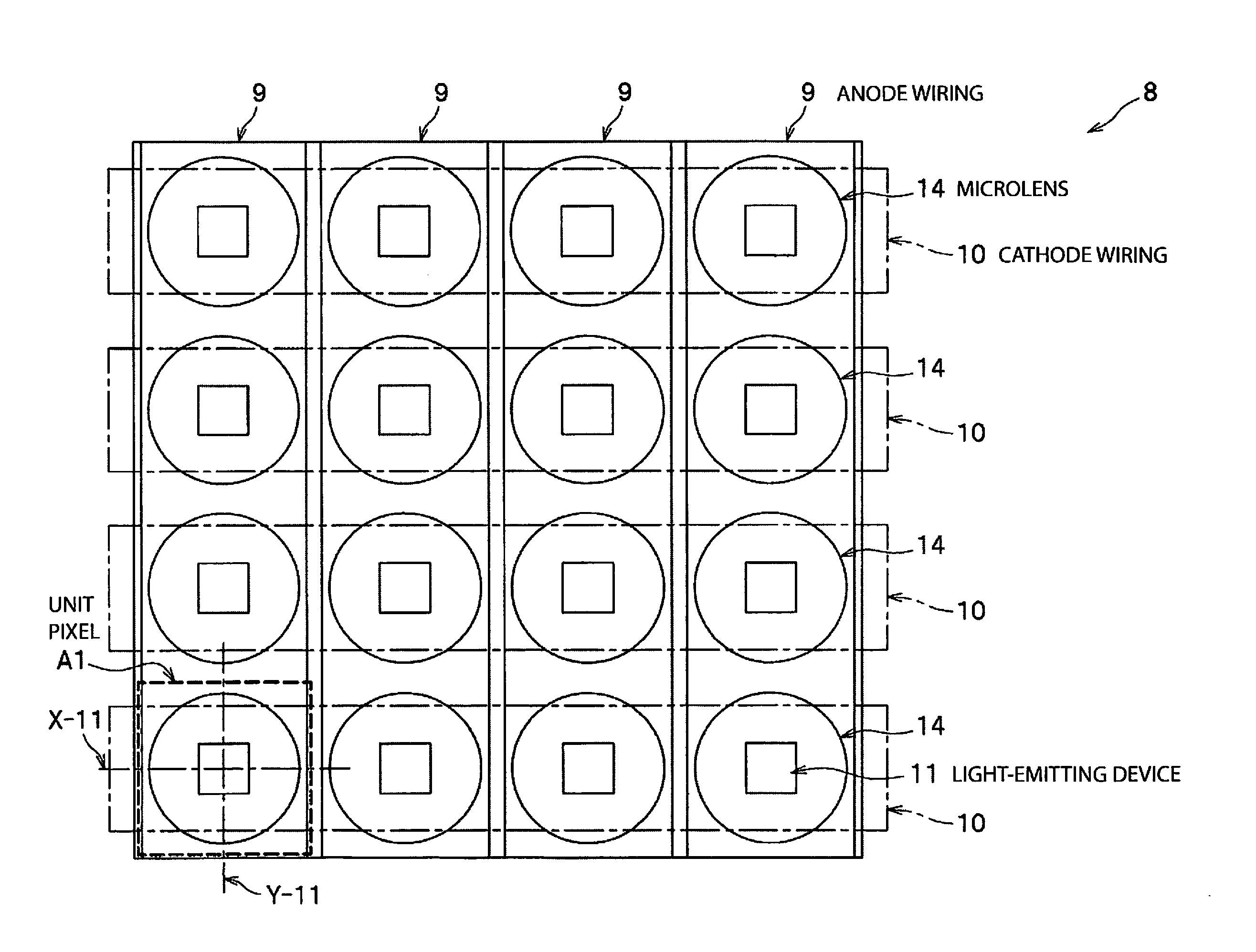
[0103]In the First Embodiment described above, anode wirings 9 are formed in contact with light-emitting devices 11 to enhance heat diffusion. External light 49 such as sun light enters head up display apparatus 100, is guided by concave mirror 50 and planar mirror 51 to reach light-emitting device array 8, and is concentrated by each microlens 14 on light-emitting device array 8 to reach a corresponding light-emitting device 11. Heat locally generated in light-emitting device 11 is diffused in the entire light-emitting device 11 to thereby prevent device performance deterioration of light-emitting device 11.

[0104]However, when concentrated external light 49 is reflected on anode wirings 9 and is absorbed, for example, by microlenses 14 or the like, the temperature environment around light-emitting devices 11 might be changed to cause device deterioration.

[0105]Hence, in this embodiment, black resist 52 is further applied to upper layers of anode wirings 9 formed in con...


PUM


Abstract

A light-emitting panel includes semiconductor light-emitting devices each having a first surface and a second surface, the first surface being placed on a surface of a substrate; lenses each provided in close contact with at least a center portion of the second surface of a corresponding semiconductor light-emitting device. The light-emitting panel further includes a connection wiring being in contact with a region around the center portions while having openings corresponding to the respective center portions.

Description

CROSS REFERENCE TO RELATED APPLICATIONS[0001]This application claims priority based on 35 USC 119 from prior Japanese Patent Application No. 2012-014766 filed on Jan. 27, 2012, entitled “LIGHT-EMITTING PANEL AND HEAD UP DISPLAY INCLUDING THE SAME”, the entire contents of which are incorporated herein by reference.BACKGROUND OF THE INVENTIONField of the Invention[0002]This disclosure relates to a light-emitting panel including a light-emitting device array with microlenses and a head up display including the light-emitting panel.[0003]Light-emitting devices are conventionally classified into a spontaneous light-emitting device and a non-spontaneous light-emitting device from a viewpoint of the light-emitting mechanism. The spontaneous light-emitting device includes a light emitting diode (LED), an organic electroluminescent (EL) device, an inorganic EL device, and the like, while the non-spontaneous light-emitting device includes a liquid crystal (LC) device and the like.[0004]An ima...

Claims


Application Information

Patent Timeline
Patent Type & Authority Applications(United States)
IPC IPC(8): F21V5/00
CPCF21V5/007G02B2027/0118G02B27/01G02B3/0006H01L2224/48091H01L2224/48227H01L2224/48472H01L2224/73265H01L2924/00014H01L2924/00
Inventor TANAKA, SATOSHITANIGAWA, KENICHI
Owner OKI DATA CORP
Learn More