Method for manufacturing a gate-control diode semiconductor device

a gate-control diode and semiconductor technology, applied in the direction of semiconductor devices, diodes, electrical devices, etc., can solve the problems of increasing device current and device breakdown, and achieve the effect of reducing chip power consumption, reducing leakage current and ss valu

Inactive Publication Date: 2013-07-11
FUDAN UNIV
View PDF0 Cites 9 Cited by
  • Summary
  • Abstract
  • Description
  • Claims
  • Application Information

AI Technical Summary

Benefits of technology

[0007]In view of this, the present invention aims at providing a method for manufacturing a gate-control diode semiconductor device capable of reducing the leakage current and the SS value so as to reduce the chip power consumption.

Problems solved by technology

Usually, both triodes can be magnified mutually, which may cause the increase of the device current and further cause the breakdown of the device in severe cases.

Method used


Image

  • Method for manufacturing a gate-control diode semiconductor device
  • Method for manufacturing a gate-control diode semiconductor device
  • Method for manufacturing a gate-control diode semiconductor device

Examples


Embodiment Construction

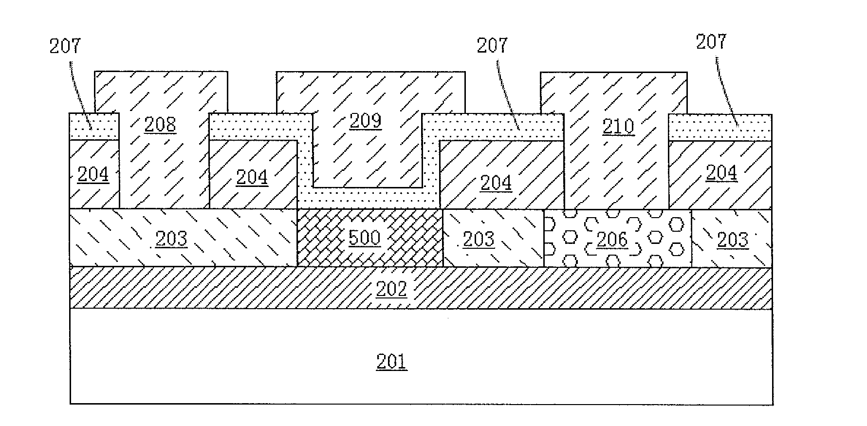
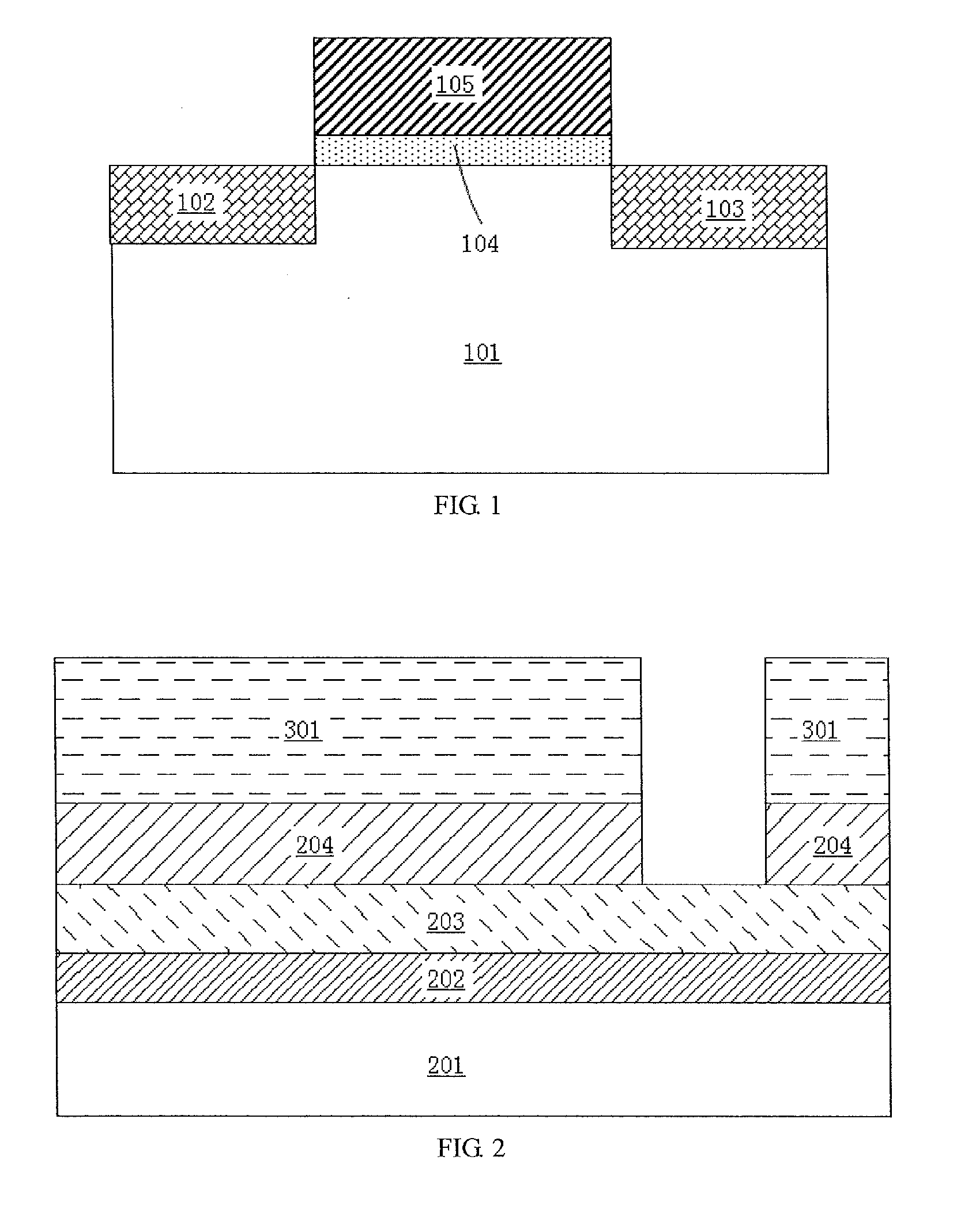
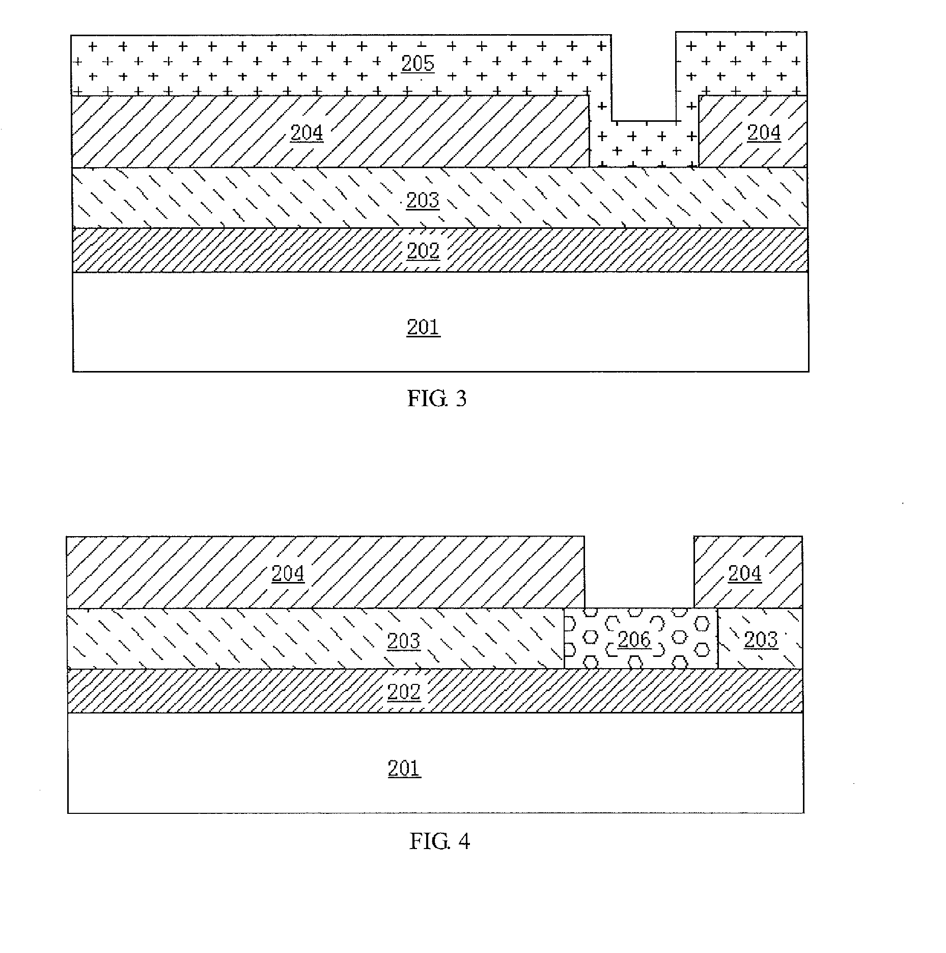
[0029]An exemplary embodiment of the present invention is further detailed herein by referring to the drawings. In the drawings, the thicknesses of the layers and regions are either zoomed in or out for the convenience of description, so it shall not be considered as the true size. Although these drawings cannot accurately reflect the true size of the device, they still reflect the relative positions among the regions and composition structures completely, especially the up-down and adjacent relations.

[0030]The reference diagrams are the schematic diagrams of the idealized embodiments of the present invention, so the embodiments shown in the present invention shall not be limited to specific shapes in areas shown in the drawings, while they shall include the obtained shapes such as the deviation caused by manufacturing. For instance, curves obtained through etching are often bent or rounded, while in the embodiments of the present invention, they are all presented in rectangles, and...


PUM


Abstract

This invention belongs to semiconductor device manufacturing field and discloses a method for manufacturing a gate-control diode semiconductor device. When the gate voltage is relatively high, the channel under the gate has an n type and the device has a simple gate-control pn junction structure; by way of controlling the effective n-type concentration of the ZnO film through back-gate control, inverting the n-type ZnO into p-type through the gate and using NiO as a p-type semiconductor, an n-p-n-p doping structure is formed. The present invention features capacity of manufacturing gate-control diode devices able to reduce the chip power consumption through the advantages of a high driving current and small sub-threshold swing, is especially applicable to the manufacturing of reading & writing devices having flat panel displays & phase change memory, and semiconductor devices based on flexible substrates.

Description

CROSS-REFERENCE TO RELATED APPLICATION[0001]This application claims priority to Chinese Patent Application No. CN 201210001675.9 filed on Jan. 5, 2012, the entire content of which is incorporated by reference herein.BACKGROUND OF THE INVENTION[0002]1. Technical Field[0003]The present invention belongs to the technical field of semiconductor device manufacturing, relates to a method for manufacturing a semiconductor device, and more especially, to a method for manufacturing a gate-control diode semiconductor device.[0004]2. Description of Related Art[0005]The Metal-Oxide -Semiconductor Field Effect Transistor (MOSFET) is a kind of field effect transistor capable of being widely used in the analog circuits and digital circuits, of which the basic structure is as shown in FIG. 1, including a silicon substrate 101, a gate insulation layer 104 and a gate conductive layer 105 formed on the silicon substrate 101, wherein a drain region 102 and a source region 103 are arranged on both sides...

Claims


Application Information

Patent Timeline
Patent Type & Authority Applications(United States)
IPC IPC(8): H01L21/34
CPCH01L29/66356H01L29/22H01L29/7391
Inventor WANG, PENGFEICAO, CHENGWEISUN, QINGQINGZHANG, WEI
Owner FUDAN UNIV
Why Eureka
Try Eureka