Method of design of control circuit in static storage in LCD drive chipset

A technology for static memory and driving chips, applied in static indicators, cathode ray tube indicators, instruments, etc., can solve the problems of complex circuit structure and high chip power consumption, reduce chip power consumption, reduce processing time, and reduce line consumption. The effect of the number of scan operations

Inactive Publication Date: 2006-07-19
NORTHWESTERN POLYTECHNICAL UNIV
View PDF0 Cites 3 Cited by
  • Summary
  • Abstract
  • Description
  • Claims
  • Application Information

AI Technical Summary

Problems solved by technology

[0005] In order to overcome the disadvantages of complex circuit structure and high chip power consumption in the prior art, the present invention provides a method for designing a control circuit of a static memory in a liquid crystal display driver chip

Method used


Image

  • Method of design of control circuit in static storage in LCD drive chipset
  • Method of design of control circuit in static storage in LCD drive chipset
  • Method of design of control circuit in static storage in LCD drive chipset

Examples


Embodiment Construction

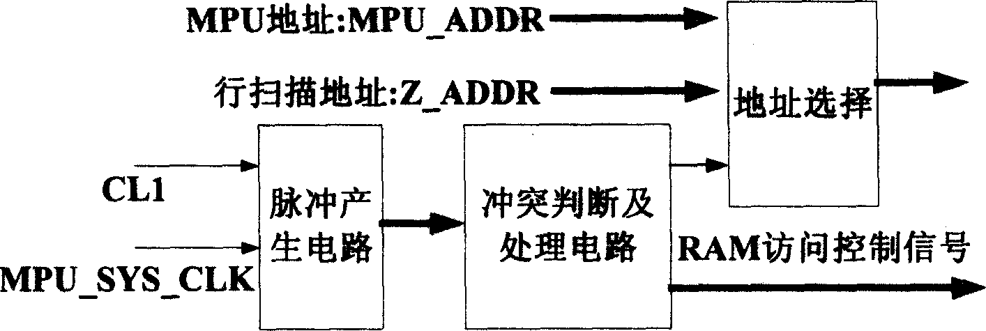
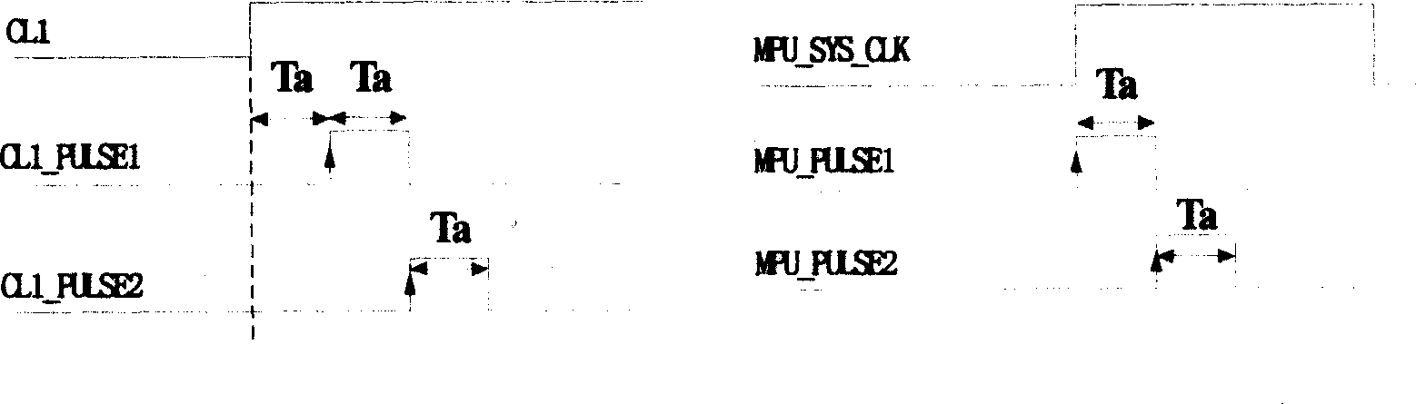
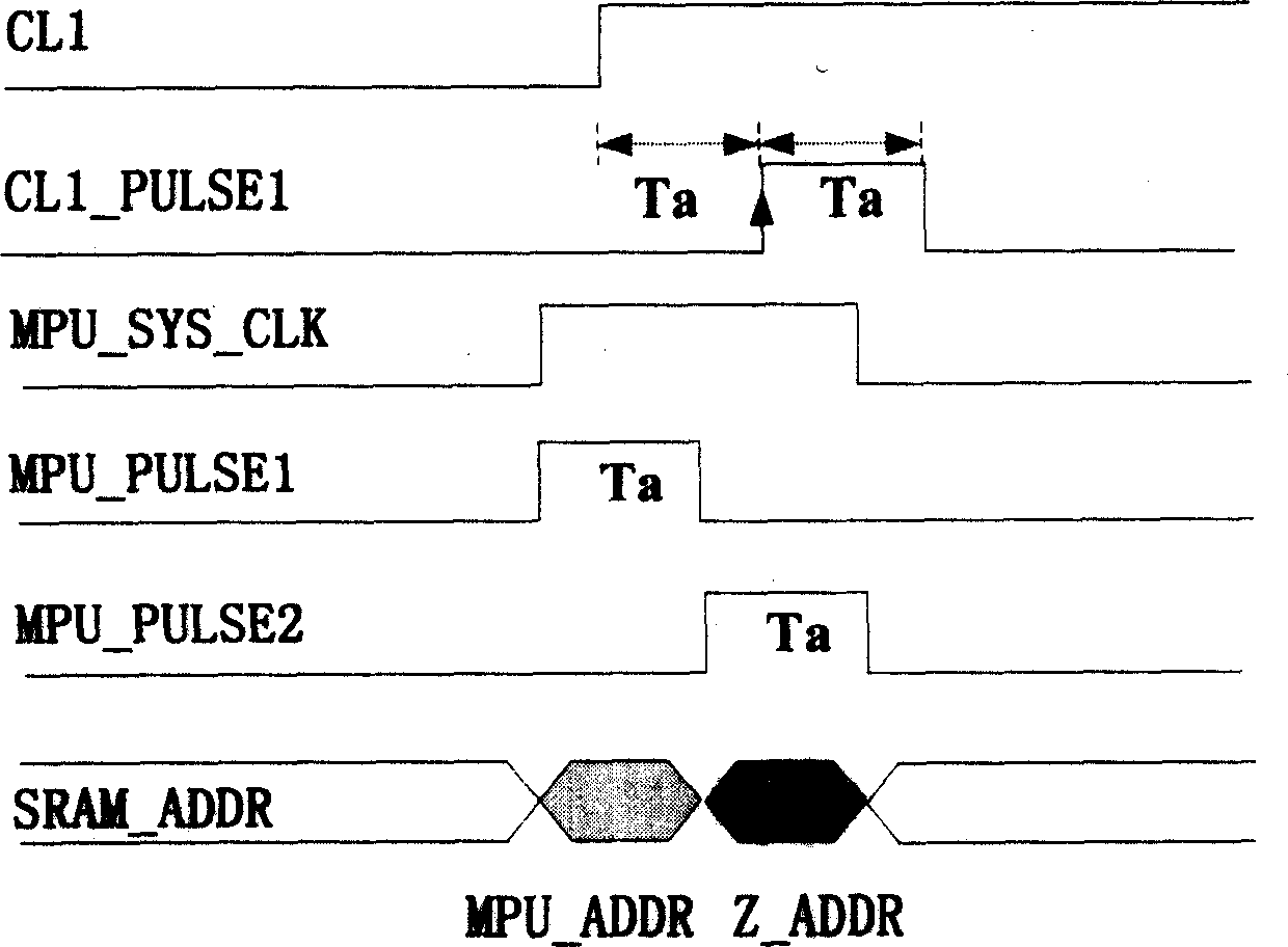
[0024] refer to Figure 1~2 In the present invention, the row scan clock CL1 and the MPU system clock MPU_SYS_CLK are used as the basic operation clocks, and each basic operation clock generates two sub-control signals with a pulse width of Ta when its rising edge arrives.

[0025] In order to ensure that the read and write operation of the MPU takes precedence over the row scan operation, the sub-control signal generated by CL1 is output after a delay of Ta. These two sub-control signals represent two time operation areas respectively. When the MPU_PULSE1 signal does not fall between the rising edge of CL1 and the falling edge of CL1_PULSE1, no timing conflict occurs; otherwise, it is determined that a timing conflict occurs. The first sub-control signal CL1_PULSE1 generated by the rising edge of the line scan signal CL1 is used as the operation area of ​​the line scan, and all the control signals required for the line scan are generated in this operation area, and the line ...


PUM


Abstract

The invention discloses a control circuit designing method of an electrostatic memory of liquid crystal driving chip. It uses the line scanning clock CL1 and MPU system clock SYS CLK as basic clocks, each basic clock generates two operating areas and each operating area generates a visit control signal, so that any operating area can finish a visit storage operation. When the line scanning operation dose not has the time sequence dash with the MPU read-and-write operation, they finish all of the operation on the first operation area; when the line scanning operation has the time sequence dash with the MPU read-and-write operation, the first operating order continuously finishes the operation on the first operation area, and the rear operating order finishes the operation on the second operation area. When it has the time sequence dash, the line scanning operation and the MPU read-and-write operation can be finished in a period of the MPU system clock.

Description

technical field [0001] The invention relates to a method for designing a control circuit of a memory, in particular to a method for designing a control circuit of a static memory in a liquid crystal display drive chip. Background technique [0002] refer to Image 6 , Figure 7 , in the liquid crystal display driving circuit chip, in order to reduce the number of data exchanges with the MPU, so as to reduce the burden on the MPU and the power consumption of the chip, it is usually necessary to have a built-in SRAM to store the image display data of one frame. There are two situations for accessing and data manipulation of the built-in SRAM, one is the read and write operation of the MPU to the SRAM to update the image display data; the other is to output the image display data stored in the SRAM to the output latch unit line by line, And drive the display through the Source Driver to display a color image (hereinafter referred to as line scan operation). In order to save t...

Claims


Application Information

Patent Timeline
IPC IPC(8): G09G3/36G09G5/39G09G3/20G02F1/133
Inventor 魏廷存高德远樊晓桠张盛兵罗旻王党辉
Owner NORTHWESTERN POLYTECHNICAL UNIV
Why Eureka
Try Eureka