Monolithic integration method of grating light modulator and active matrix driving circuit

A technology of optical modulators and driving circuits, applied in chemical instruments and methods, circuits, instruments, etc., to achieve the effects of increasing circuit transmission rate, reducing signal noise, and reducing area

Inactive Publication Date: 2009-03-25
CHONGQING UNIV
View PDF1 Cites 7 Cited by
  • Summary
  • Abstract
  • Description
  • Claims
  • Application Information

AI Technical Summary

Problems solved by technology

Moreover, when the grating light modulator array driven by the passive matrix performs progressive scanning, only one row can be displayed at each moment, and the light utilization rate is only 1 / N (N is the number of rows)
These all limit the development of GLM devices for high-resolution, high-definition projection displays

Method used


Image

  • Monolithic integration method of grating light modulator and active matrix driving circuit
  • Monolithic integration method of grating light modulator and active matrix driving circuit
  • Monolithic integration method of grating light modulator and active matrix driving circuit

Examples


Embodiment Construction

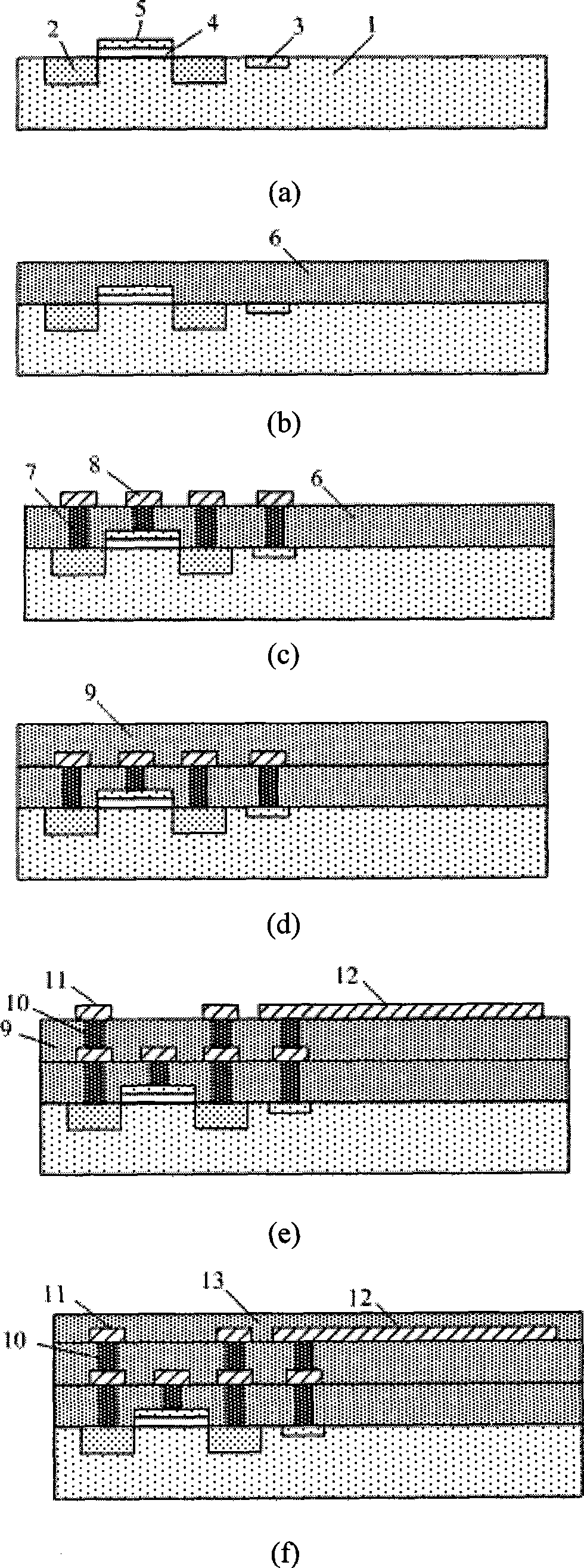
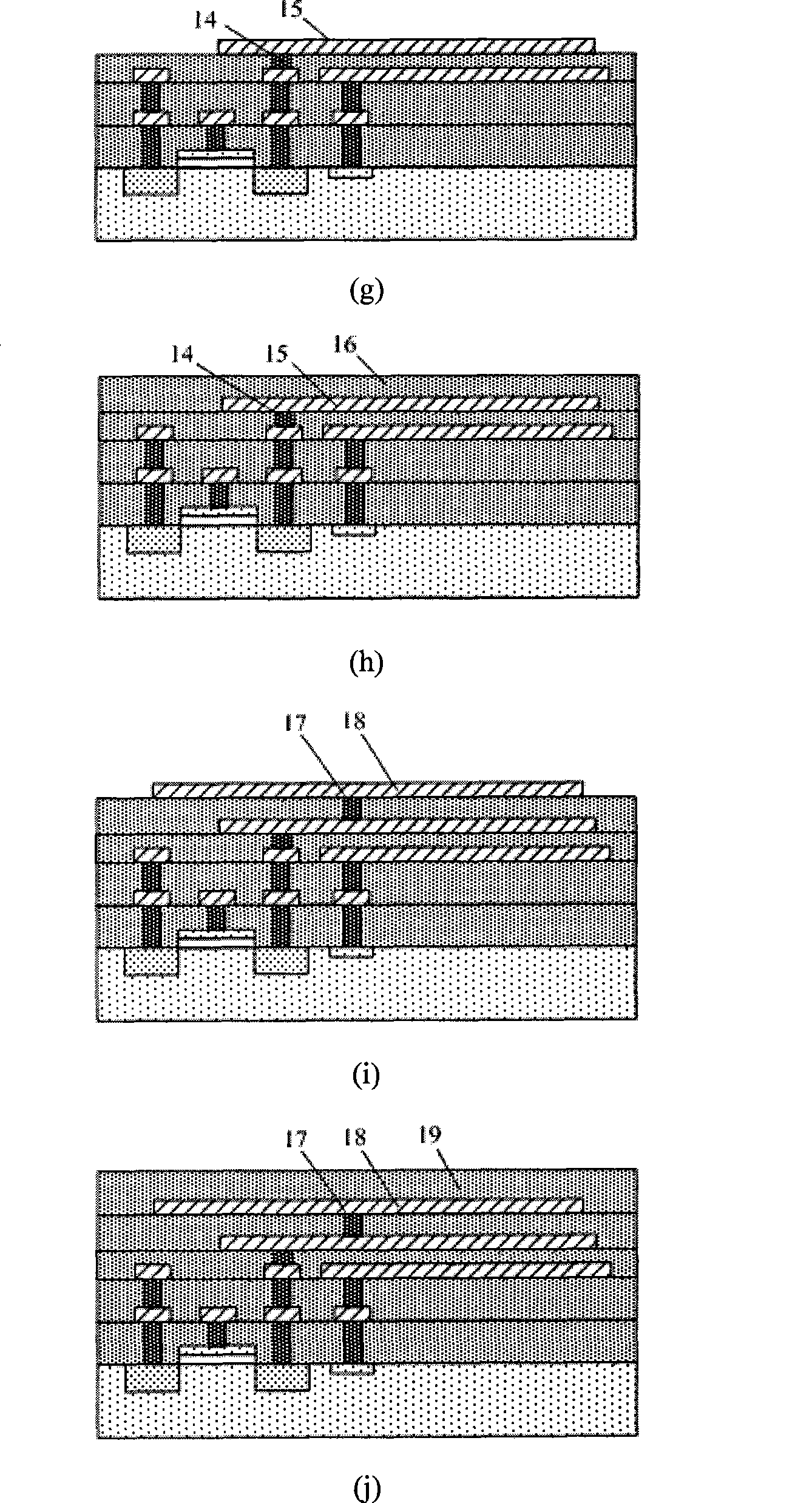
[0024] Below in conjunction with accompanying drawing and embodiment the present invention is further described:

[0025] The structure of the grating modulator with an active matrix driving circuit is based on the existing IC technology, and is a MEMS device that is layered on a silicon chip. Contains the following structures:

[0026] A silicon substrate on which an active matrix drive circuit is formed by a CMOS process;

[0027] A lower electrode of the grating modulator located above the active matrix driving circuit, on which an insulating layer is deposited;

[0028] An upper movable grating is located on the insulating layer and supported by four sides connected with cantilever beams.

[0029] As the voltage applied between the upper movable grating and the lower electrode is different, the distance between the upper movable grating and the lower electrode is variable, forming a rectangular groove phase grating with adjustable depth, which produces a modulation effec...


PUM


Abstract

The invention provides a monolithic integration method for a grating optical modulator and an active matrix drive circuit, which is combined with the processing technique of monolithic integration of an MEMS device and a CMOS circuit, utilizes the CMOS circuit to process the active matrix drive circuit at first and then utilizes the low-temperature micromechanical manufacturing technique to obtain the MEMS grating optical modulator, so as to realize monolithic integration of the MEMS grating optical modulator which is formed by upper movable gratings supported on lower electrodes and the lower active matrix drive circuit. The grating optical modulator processed by the technique can project and display with high definition and high resolution.

Description

technical field [0001] The invention belongs to the technical field of process design for monolithic integration of a grating light modulator and an active matrix drive circuit. Process the grating light modulator to achieve monolithic integration of the two in the vertical direction, thereby significantly improving the performance of the grating light modulator as a projection display device. Background technique [0002] In recent years, with the continuous development of MEMS technology, the requirements for future MEMS devices are: miniaturization and integration; low power consumption and low cost; high precision and long life; multi-function and intelligence. The monolithic integration of MEMS and CMOS integrated circuits can meet the above requirements. The realization of monolithic integration is the key to realizing the intelligence of MEMS devices, especially the monolithic integration of MEMS technology is one of the key technologies for the realization of system...

Claims


Application Information

Patent Timeline
IPC IPC(8): G02B26/08B81C5/00B81C99/00
Inventor 张智海金珠张洁王宁韦玮
Owner CHONGQING UNIV
Why Eureka
Try Eureka