
Method for purifying alkaline treatment fluid for semiconductor substrate and a purification apparatus

a technology of alkaline treatment liquid and purification apparatus, which is applied in the direction of filtration separation, silicon compounds, separation processes, etc., can solve the problems of deterioration of electric characteristics of devices, pattern defects, and tmah aqueous solution being liable to be contaminated with metals, and it is difficult to prevent completely contamination derived from storage containers, etc., to achieve strong adsorption purification, strong adsorption performance, and high adsorption performan

Inactive Publication Date: 2013-07-11
TAMA KAGAKU IND +1
View PDF0 Cites 13 Cited by
  • Summary
  • Abstract
  • Description
  • Claims
  • Application Information

AI Technical Summary

Benefits of technology

The present invention is about a method for purifying metal impurities from an alkaline treatment liquid using a silicon carbide crystal face as an adsorption purification means. The silicon carbide crystal face has a strong adsorption ability for metal hydroxide colloid impurities in the alkaline treatment liquid. Compared to silicon, the silicon carbide crystal face has much stronger adsorption performance. The use of silicon carbide as an adsorption purification means is advantageous over silicon because silicon carbide does not dissolve in the alkaline treatment liquid, minimizing contamination. The purification effect of silicon carbide is easily achieved through a cleaning treatment with a weak acid-based cleaning agent and water rinse. The silicon carbide crystal face can be easily regenerated and can be incorporated into a multistep parallel purification mechanism. The use of silicon carbide as an adsorbent exerts excellent chemical resistance and mechanical strength, making it ideal for preparing a grainy adsorbent. The ratio of the total surface area of the grainy adsorbent to the volume of the filling liquid is large, resulting in a high removal ratio of the impurities. The present invention allows for effective removal of harmful metal elements such as iron from the alkaline treatment liquid, making ultrahigh purification treatment of a developer easier and controllable.

Problems solved by technology

However, when a commercially available product thereof was initially produced, the product contained metal impurities such as Na, Fe, Zn, Ca, Mg, Ni, Cr, Al, and Cu at concentrations of about several ppm and contained K as a metal impurity at a much higher concentration, and hence the metal impurities caused problems such as deterioration of electric characteristics of a device and pattern defects.
A TMAH aqueous solution was initially produced by a method in which an alcohol solution of tetramethylammonium chloride is caused to react with hydroxides, the resultant precipitates are removed by filtration, and the alcohol solvent is then removed (see, for example, Patent Literature 1), and hence the TMAH aqueous solution was liable to be contaminated with metals owing to dissolution of metal impurities such as Fe, Al, Ni, and Na from its production materials, production apparatus, storage containers, and the like.
However, even in the TMAH aqueous solution thus purified, highly corrosive chlorides remained, and hence it was difficult to prevent completely contamination derived from a storage container.
Among these elements, Fe is a heavy metal that causes problems such as an increase in junction current of a device, life time deterioration, and poor pressure resistance of an oxide film.
However, the production apparatus and transporting vessel therefor involve drawbacks in their materials as in the case of the above-mentioned organic strong base, and Fe may probably exist at a concentration of about 0.03 to 0.1 ppb in these chemicals for a semiconductor as well, though the standard of the Fe concentration in both commercially available chemicals has been set, over these several years, to 0.1 ppb, which is the measurement limit value measured by normal analytical means, or less.
Although the purification method in which filtration is preformed through a silicon grain-packed layer had been used for about ten years to remove Cu and Au in hydrofluoric acid in semiconductor plants, the use of the method was stopped because the influence of fluorosilicic acid that dissolved caused some problems.
It is possible to produce silicon grains having an Fe concentration of 0.1 ppm or less by a CVD fluid bed method, but the method has a disadvantage from the economical point of view.
In addition, when silicon fine grains are produced by pulverizing a silicon ingot for a semiconductor, Fe contamination derived from a pulverizer occurs, and because it is difficult to remove the Fe contamination by cleaning or the like, even an Fe concentration of 0.1 ppm cannot be obtained by this method.
The silicon grains involve problems in their purity as described above.

Method used


Image

  • Method for purifying alkaline treatment fluid for semiconductor substrate and a purification apparatus
  • Method for purifying alkaline treatment fluid for semiconductor substrate and a purification apparatus
  • Method for purifying alkaline treatment fluid for semiconductor substrate and a purification apparatus

Examples


example 1

[0084]Two silicon carbide single crystal (6H) wafers each having a diameter of 75 mm were used to take preliminarily atomic force microscope (AFM) images of the mirror surfaces of these wafers. After that, the mirror surfaces were positioned so as to face to each other, and an adsorbing plate laminate having a slit gap with a gap of 0.5 mm of Example 1 was formed in the same manner as that in the Fe adsorption purification experiment described previously.

[0085]Radioactive 59Fe was added into the above-mentioned 5-wt % choline aqueous solution, yielding a test liquid having a radioactive 59Fe concentration of 100 ppt, and the adsorbing plate laminate of Example 1 and the test liquid were used to carry out an Fe adsorption purification experiment under room temperature in accordance with the same procedure as that in the Fe adsorption purification experiment described previously, thereby calculating the remaining ratio of radioactive 59Fe in the test liquid.

[0086]After that, the insid...

example 2

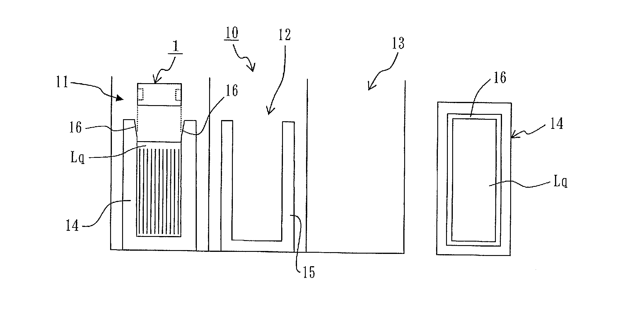
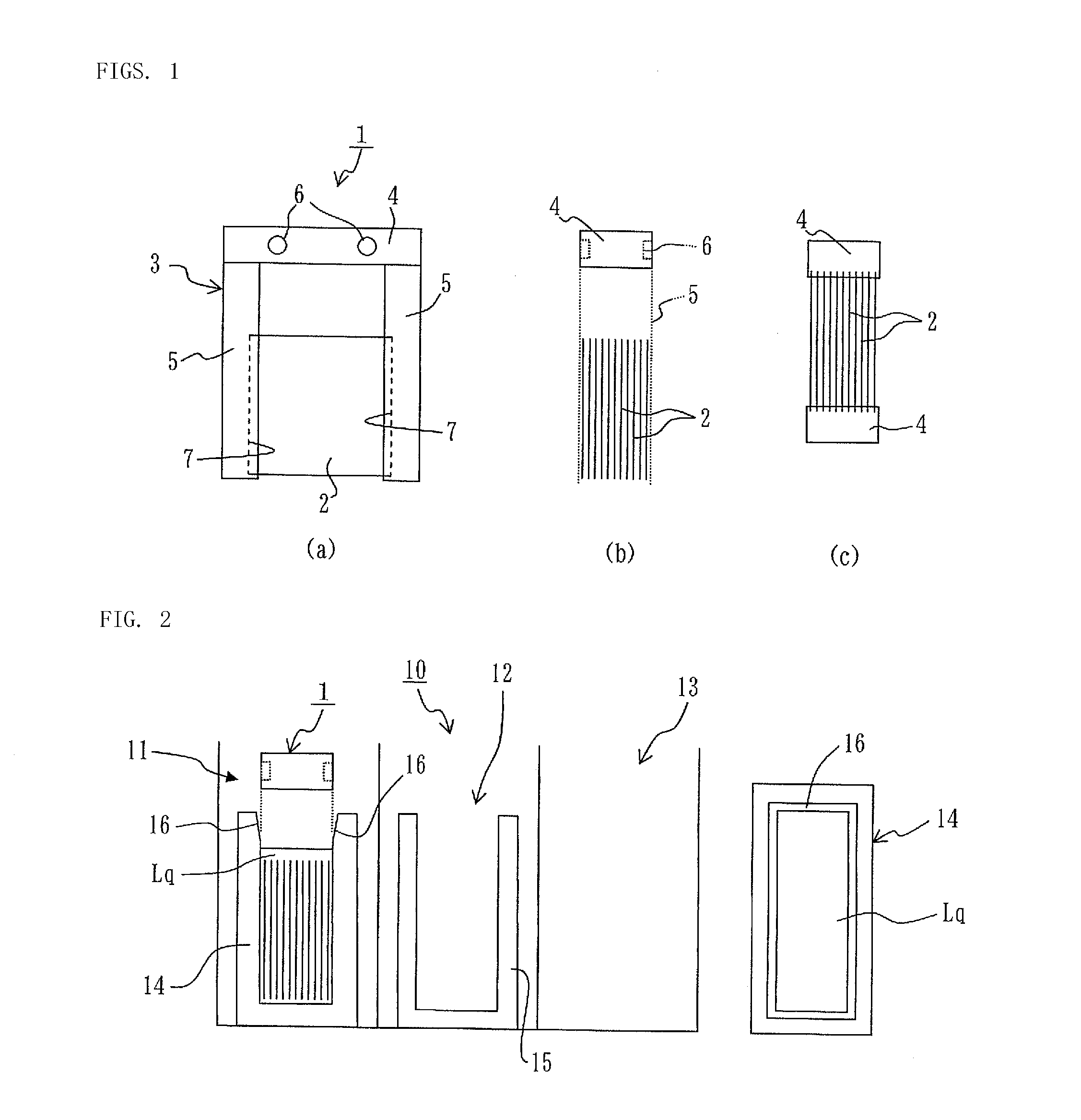
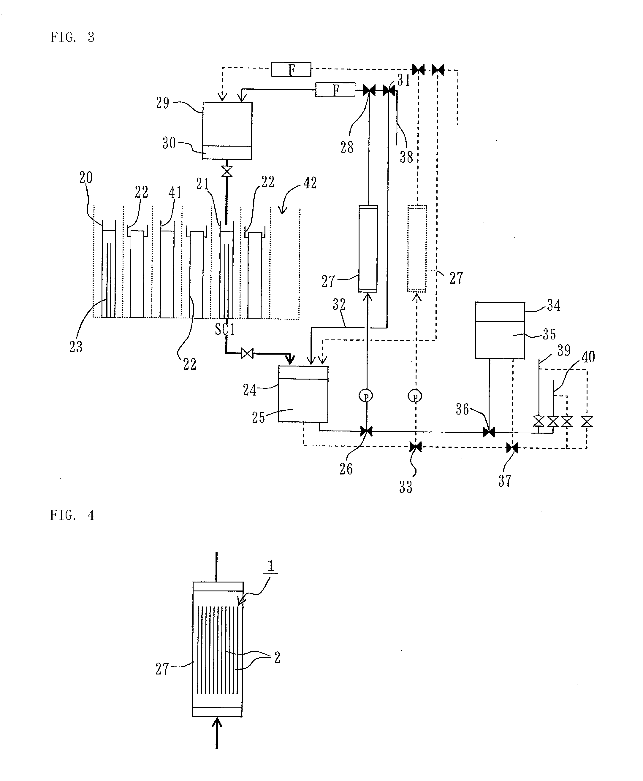
[0091]Based on the findings of the Example 1, an adsorbing plate laminate 1 illustrated in FIGS. 1(a) to 1(c) was constructed as adsorption purification means for an alkaline treatment liquid. The adsorbing plate laminate 1 is constituted of a set of 11 adsorbing plates 2 each having a thin plate shape cut out from a CVD polycrystal dummy wafer (K≈0.3, front and back surfaces with good hydrophilicity) having a thickness of 0.6 mm by a laser process so as to have a size of 100 mm by 102 mm and a holding cassette 3 made of a fluororesin (PTFE) for holding the adsorbing plates 2 with a predetermined interval (usually 0.8 to 3.0 mm, preferably 1 to 2 mm) to each other, with a parallel state to each other, with the state of facing to each other. Further, the holding cassette 3 is constituted of a cassette ceiling portion 4 having a recessed portion 6 for connecting to a robot arm (not shown) for transporting and positioning the adsorbing plate laminate 1 and a pair of cassette arm portio...

example 3

[0103]In order to use high-purity silicon carbide grains each having a grain diameter of 0.2 to 1.2 mm (GNF-CVD manufactured by Pacific Rundum Co. Ltd.), which are a single crystal material, as an adsorption purification agent, the silicon carbide grains were dipped and cleaned preliminarily in each of a choline stock solution and nitric acid for several days. After that, a fluororesin column having an inner diameter of 20 mm and a length of about 120 mm was filled with 60 g of the cleaned silicon carbide grains (an apparent volume of about 30 mL), thereby constituting an adsorbent-packed column. 500 mL each of various liquids were passed through the column, starting from a 7-wt % nitric acid aqueous solution, followed by ultrapure water, 2-wt % hydrofluoric acid / 1-wt % hydrogen peroxide aqueous solution, and ultrapure water, in the stated order, and then a purification experiment of a test liquid was performed.

[0104]Further, a 4 wt % choline aqueous solution (choline stock solution...


PUM

PropertyMeasurementUnit
surface reflectanceaaaaaaaaaa
areaaaaaaaaaaa
grain diameteraaaaaaaaaa

Abstract

Provided are a purification method and purification apparatus for an alkaline treatment liquid for a semiconductor substrate, which use adsorption purification means that can purify various alkaline treatment liquids to be used for treating semiconductor substrates for various purposes so as to have an ultrahigh purity, in particular, an Fe concentration in a ppq region, and that is excellent in chemical resistance and mechanical strength. The adsorption purification means is purification means for an alkaline treatment liquid for treating a semiconductor substrate for various purposes at the time of producing, for example, a semiconductor substrate or a semiconductor device. In the purification method and purification apparatus for an alkaline treatment liquid for a semiconductor substrate, an alkaline treatment liquid is brought into contact with silicon carbide crystal surfaces in the absorption purification means, for example, an alkaline treatment liquid is allowed to flow through a gap between adsorbing plate laminates (2) whose both surfaces are CVD silicon carbide surfaces, thereby removing metal impurities contained in the alkaline treatment liquid through adsorption of the metal impurities to the silicon carbide crystal surfaces.

Description

TECHNICAL FIELD[0001]The present invention relates to a method for purifying an alkaline treatment liquid which is used for treating a semiconductor substrate for various purposes and a purification apparatus, for example, when the semiconductor substrate is produced or when a semiconductor device or the like is produced by using the semiconductor substrate, and more specifically, to a method for purifying an alkaline treatment liquid for a semiconductor substrate, by which concentrations of metal impurities, in particular, iron (Fe), which are contained in very small amounts in various alkaline treatment liquids to be used for treating the semiconductor substrate, contaminate a surface of the semiconductor substrate, and are harmful to a device or the like to be produced by using the semiconductor substrate, can be reduced to a ppq (one thousandth of ppt) region, if necessary, and to a purification apparatus used for carrying out the above-mentioned purification method.BACKGROUND A...

Claims


Application Information

Patent Timeline
Patent Type & Authority Applications(United States)
IPC IPC(8): B01J20/10
CPCB01J20/0251H01L21/02052B01J20/28035H01L29/1608B01J20/10C02F1/28H01L21/302
Inventor MURAOKA, HISASHICHO, TOSHITSURA
Owner TAMA KAGAKU IND
Learn More