Lithographically enhanced edge determination

a technology of enhanced edge and lithography, applied in the field of lithographically enhanced edge determination, can solve the problems of increased computation complexity, inconvenient use, and increased computation time, and achieve the effect of reducing the cost of production, and increasing the complexity of computations

Active Publication Date: 2013-05-30
SYNOPSYS INC
View PDF1 Cites 24 Cited by
  • Summary
  • Abstract
  • Description
  • Claims
  • Application Information

AI Technical Summary

Benefits of technology

[0017]Furthermore, the difference between the modified target pattern and the estimated target pattern may be the maximum difference between the modified target pattern and in a set of estimated target patterns produced during photolithographic processes at one or more image planes using the mask pattern the object plane.

Problems solved by technology

Unfortunately, it is increasingly difficult to design and manufacture photo-masks.
These trends have significantly increased the complexity of the computations necessary to determine the mask patterns (to which the photo-masks correspond), with a commensurate impact on computation time, processing requirements, and expense.
Furthermore, due to the wave nature of light, as dimensions approach sizes comparable to the wavelength of the light used in the photolithography processes, the resulting wafer patterns deviate from the corresponding photo-mask patterns and are accompanied by unwanted distortions and artifacts.
While these techniques may ensure that the wafer pattern is printed more accurately, determining the pre-distorted mask patterns is increasingly difficult, thereby exacerbating the computational complexity and the associated problems.
However, the integrated-circuit designers usually only consider logic requirements and electrical characteristics when generating the target patterns.
As a consequence, the polygons in the target patterns may not be lithographically optimal, i.e., they may result in large variations in the wafer patterns produced during the photolithography process.

Method used


Image

  • Lithographically enhanced edge determination
  • Lithographically enhanced edge determination
  • Lithographically enhanced edge determination

Examples


Embodiment Construction

[0033]The following description is presented to enable any person skilled in the art to make and use the invention, and is provided in the context of a particular application and its requirements. Various modifications to the disclosed embodiments will be readily apparent to those skilled in the art, and the general principles defined herein may be applied to other embodiments and applications without departing from the spirit and scope of the present invention. Thus, the present invention is not intended to be limited to the embodiments shown, but is to be accorded the widest scope consistent with the principles and features disclosed herein.

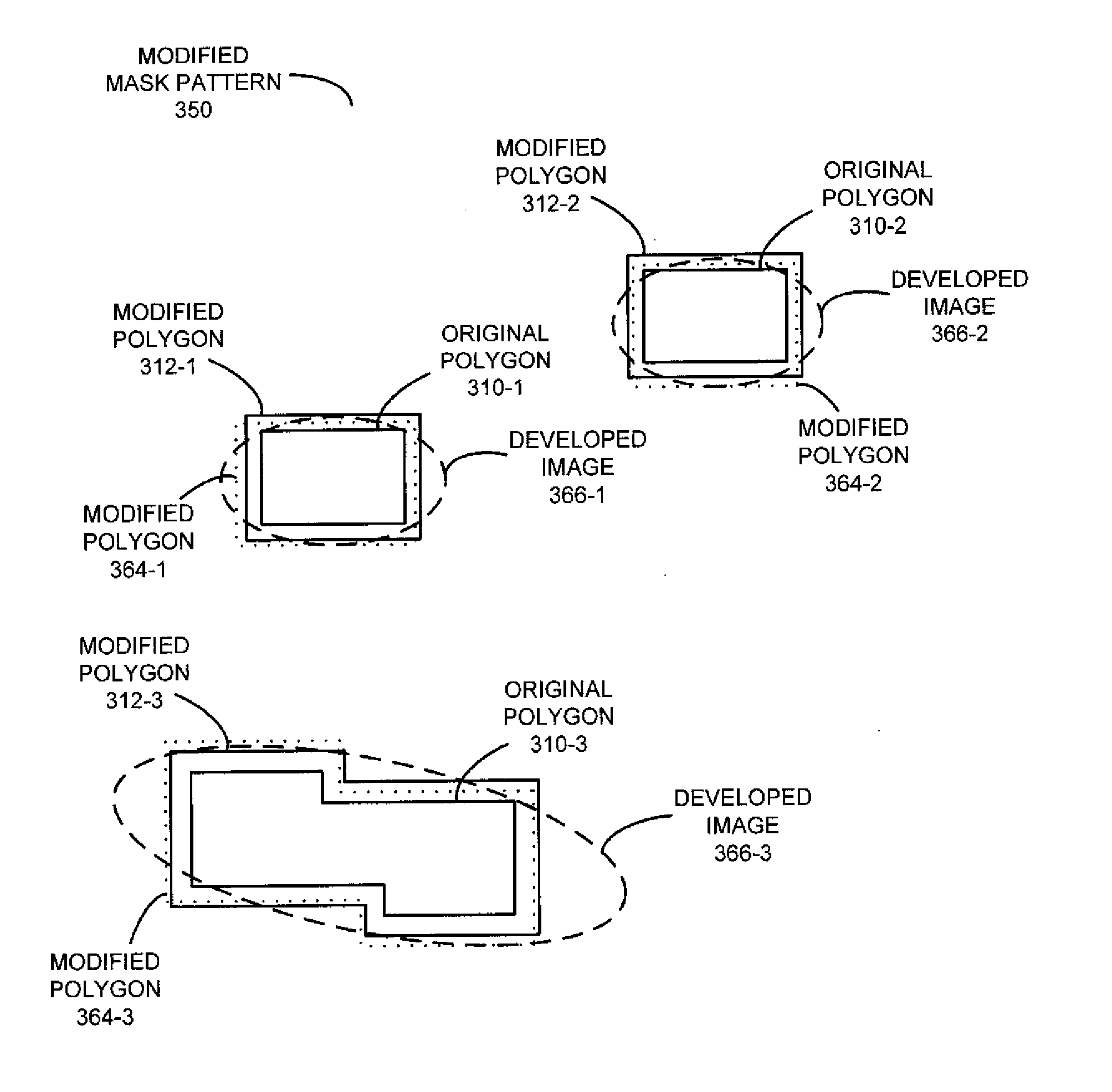
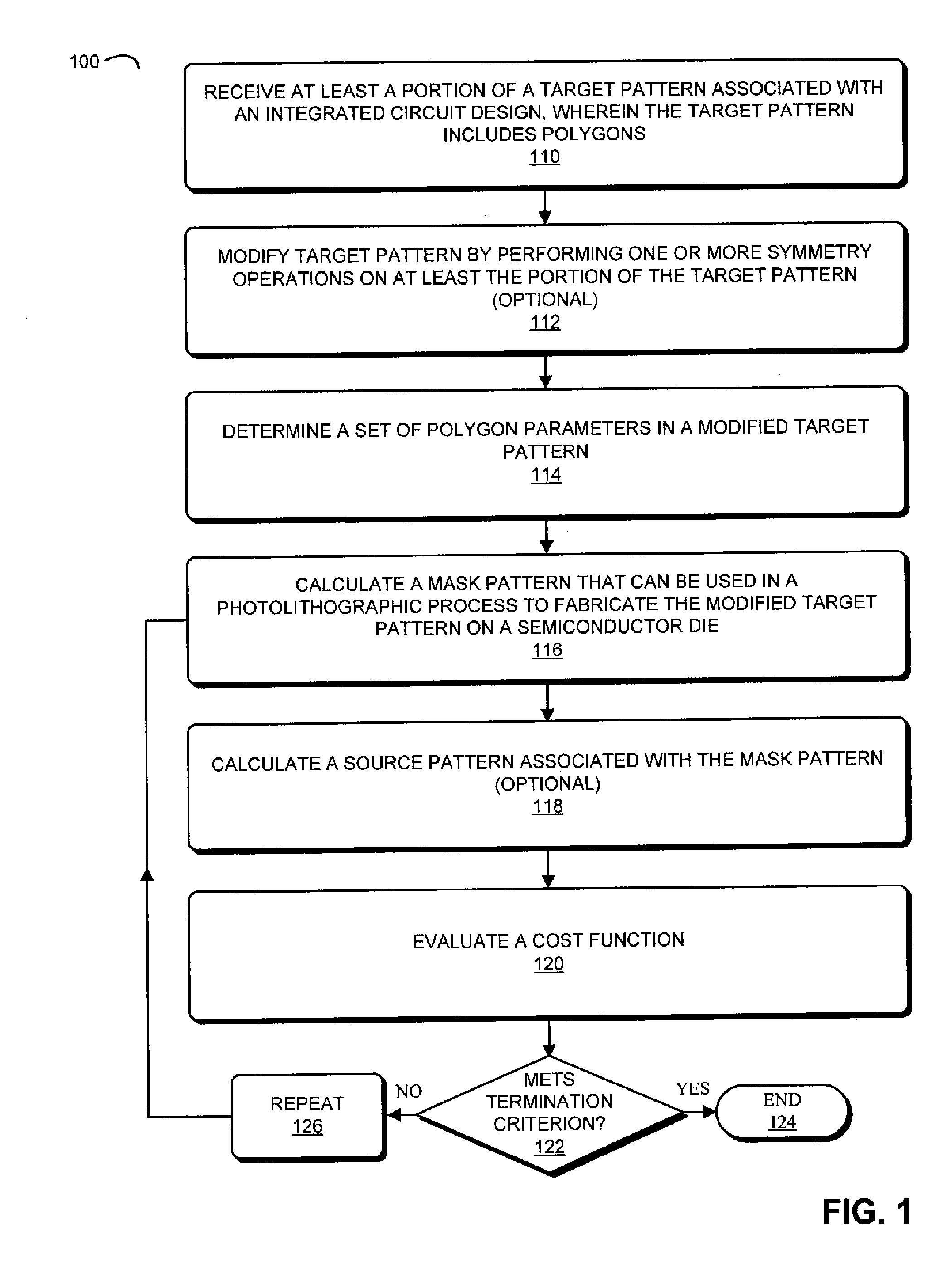
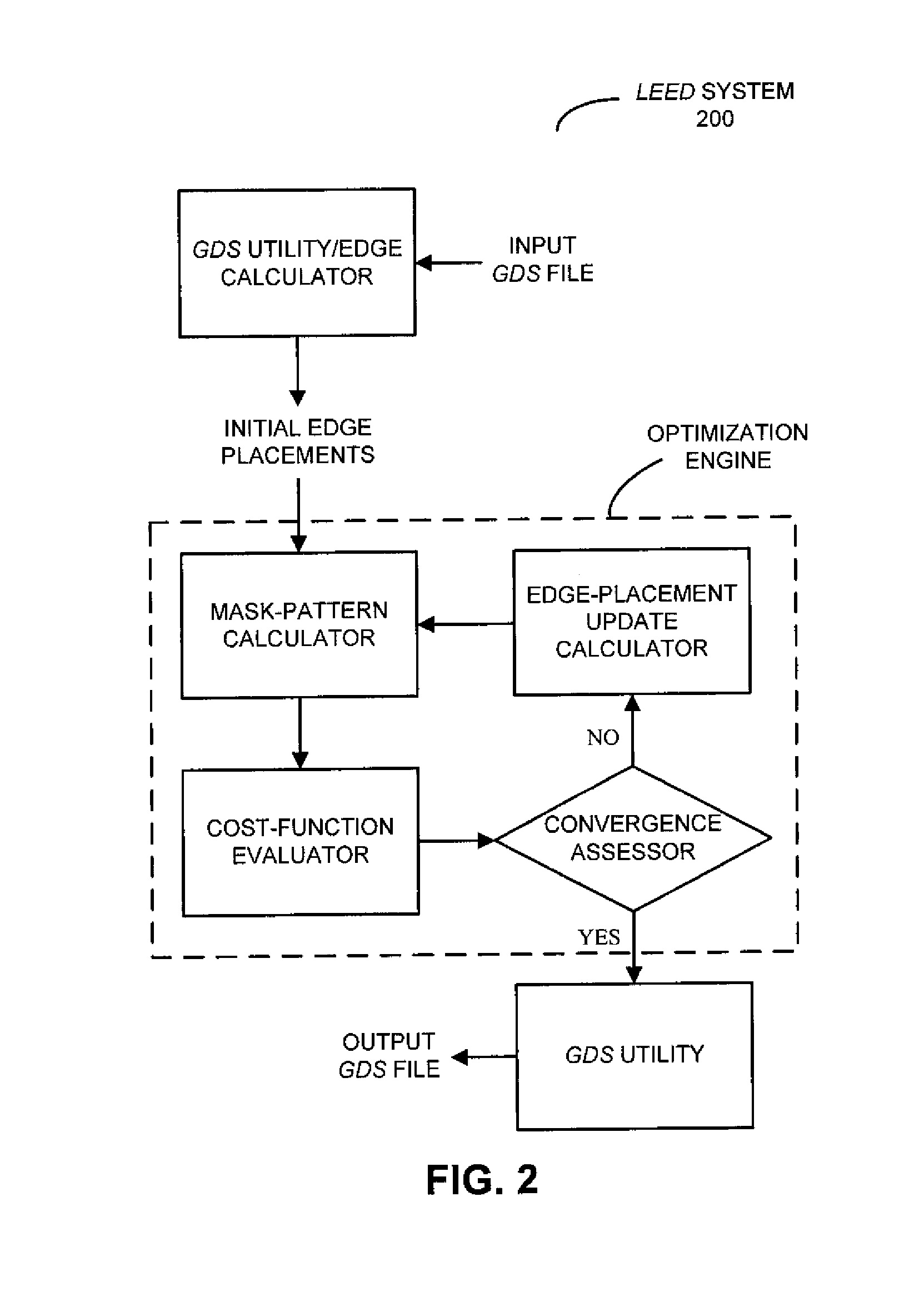
[0034]Embodiments of a computer system, a method, and a computer-program product (i.e., software) for use with the computer system are described. These devices and processes may be used to modify at least a portion of a target pattern associated with an integrated-circuit design so that polygons in the target pattern, which represent features i...


PUM


Abstract

During a calculation technique, at least a portion of a target pattern associated with an integrated-circuit design is modified so that polygons in the target pattern, which represent features in the design, result in acceptable accuracy during a photolithographic process that fabricates the target pattern on a semiconductor die. In particular, a set of polygon parameters associated with the polygons are modified, as needed, so that a cost function that corresponds to a difference between a modified target pattern and an estimated target pattern produced during the photolithographic process meets a termination criterion. A mask pattern that can fabricate the modified target pattern on the semiconductor die is calculated using an inverse optical calculation in which the modified target pattern is at an image plane of an optical path associated with the photolithographic process and the mask pattern is at an object plane of the optical path.

Description

BACKGROUND[0001]1. Field[0002]The present invention relates to systems and techniques for determining target patterns that represent integrated-circuit designs.[0003]2. Related Art[0004]Lithography processing represents an essential technology for manufacturing Integrated Circuits and Micro-Electro-Mechanical Systems (MEMS) and Nano-Electro-Mechanical Systems (NEMS). Lithographic techniques are used to define: patterns, geometries, features, shapes, etc. onto an integrated-circuit die, semiconductor wafer, or chips. These patterns are typically defined by: a set of contours, lines, boundaries, edges, curves, etc., which generally surround, enclose, and / or define the boundary of the various regions which constitute the patterns.[0005]One existing lithographic technique is photolithography, in which images defined by photo-masks are printed onto an integrated-circuit die or one or more semiconductor wafers. Unfortunately, it is increasingly difficult to design and manufacture photo-ma...

Claims


Application Information

Patent Timeline
Patent Type & Authority Applications(United States)
IPC IPC(8): G06F17/50
CPCG03F1/36
Inventor CHOW, TATUNGHU, CHANGQINGSON, DONGHWANKIM, DAVID H.CECIL, THOMAS C.
Owner SYNOPSYS INC
Why Eureka
Try Eureka