Three-dimensional integrated circuit having redundant relief structure for chip bonding section

a technology of integrated circuits and relief structures, applied in the direction of reliability increasing modifications, semiconductor/solid-state device details, testing/measurement of semiconductor/solid-state devices, etc., can solve the problems of large number of connecting members, defect occurrence, and defect in connecting members, so as to prevent the effect of reducing the yield of three-dimensional integrated circuits and reducing areas

Inactive Publication Date: 2013-05-23
PANASONIC CORP
View PDF5 Cites 13 Cited by
  • Summary
  • Abstract
  • Description
  • Claims
  • Application Information

AI Technical Summary

Benefits of technology

[0016]The three-dimensional integrated circuit according to the present invention is characterized in that the subset of the connecting members arranged in the region where the distance between the rewiring member and the chip is relatively large has a higher proportion of connecting members replaceable with a subset of the redundant connecting members. As a result, the three-dimensional integrated circuit enables the redundant circuits not only to prevent decreases in the yield of three-dimensional integrated circuits caused by faulty connections among chips, but also to have further reduced areas.

Problems solved by technology

Warpage of chips leads to the following problems.
If the chips warped at the time of bonding, increase of the distances between the chips might cause a defect to occur in a connecting member.
The probability of occurrence of a defect in a connecting member is not negligible in the first place since the structure of each connecting member is fine and minute, and in addition the number of connecting members is very large.
If the chips were designed without considering possible occurrence of a faulty connection, a chip that would happen to have a faulty connection would have to be discarded as a defective product.
That is, the yield of chips would decrease by the probability of occurrence of a faulty connection.
As a result, it is difficult to further reduce the manufacturing cost of the chips.

Method used


Image

  • Three-dimensional integrated circuit having redundant relief structure for chip bonding section
  • Three-dimensional integrated circuit having redundant relief structure for chip bonding section
  • Three-dimensional integrated circuit having redundant relief structure for chip bonding section

Examples


embodiment 1

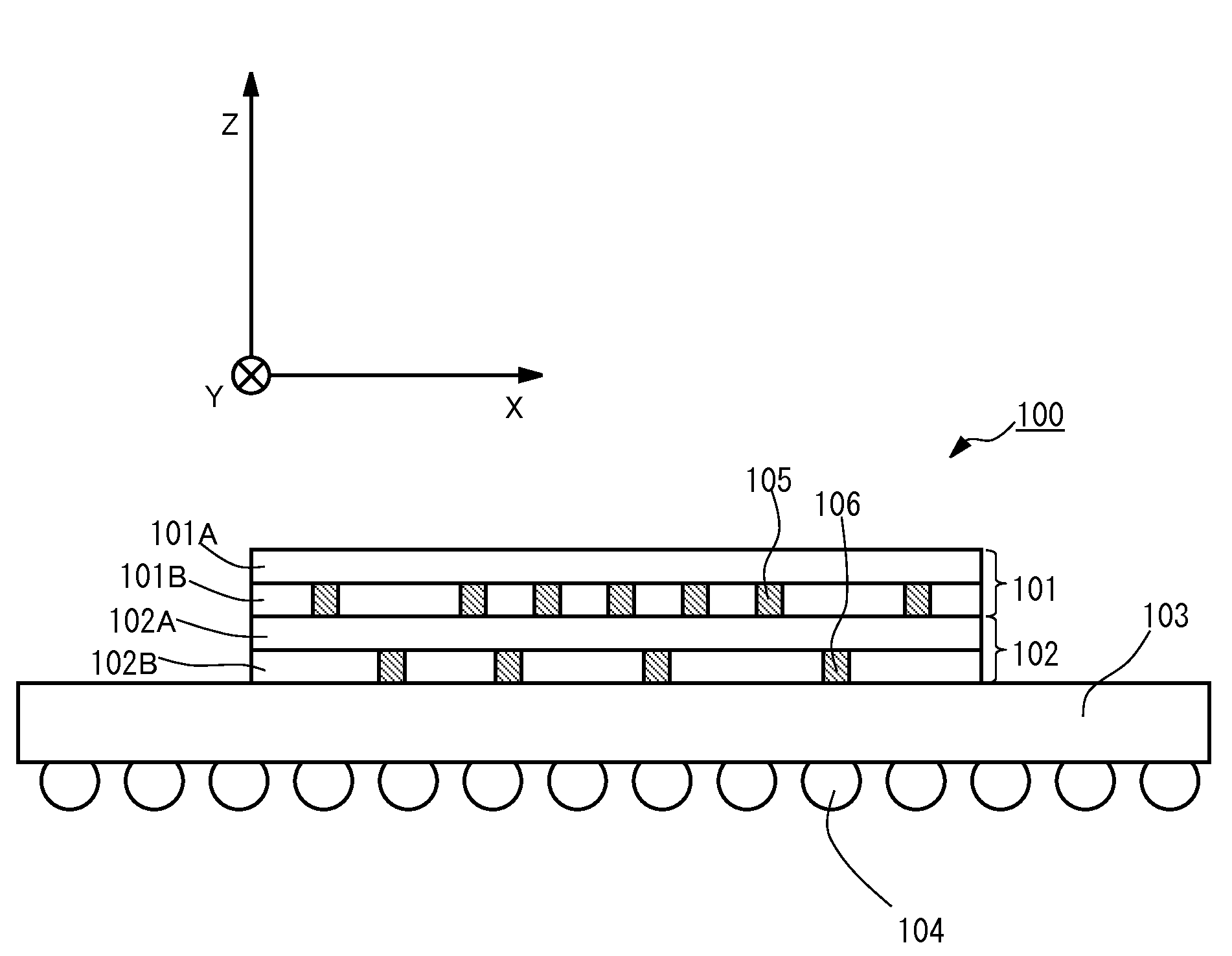
[0035]FIG. 1 is a schematic view showing a cross section of a three-dimensional integrated circuit 100 according to Embodiment 1 of the present invention. With reference to FIG. 1, the three-dimensional integrated circuit 100 includes a first chip 101, a second chip 102, an interposer 103, and bumps 104.

[0036]Each of the first chip 101 and the second chip 102 is a rectangular-plate-like member made of silicon. The first chip 101 and the second chip 102 are the same in shape and size. The first chip 101 includes a wiring layer 101A and a transistor layer 101B, and the second chip 102 includes a wiring layer 102A and a transistor layer 102B. The transistor layers 101B and 102B include a plurality of transistors. These transistors are connected to one another through the wiring layers 101A and 102A to constitute various circuits (cores). The transistor layer 101B of the first chip 101 and the wiring layer 102A of the second chip 102 are bonded to each other by an adhesive layer. As sho...

embodiment 2

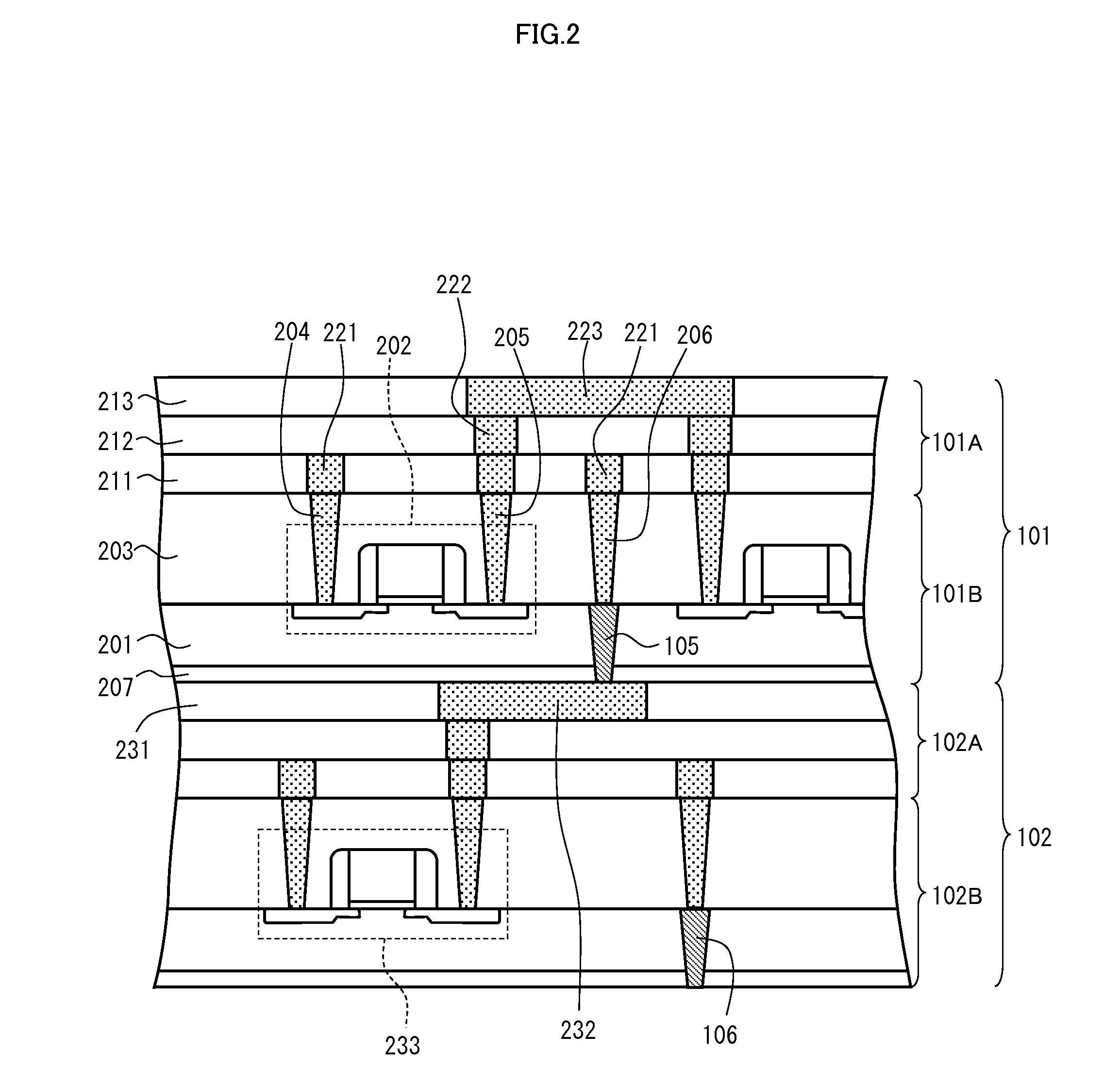
[0089]A three-dimensional integrated circuit according to Embodiment 2 of the present invention differs from that according to Embodiment 1 in arrangement of TSVs. Other components are the same as those in Embodiment 1. Accordingly, details of the other components can be found in the description of Embodiment 1.

[0090]As shown in FIG. 2, the substrate 201 of the first chip 101 is thin, and accordingly the first chip 101 warps. The same is true for the second chip 102. In Embodiment 1, the distances between the chips due to their warpage increase greater in their central region CR than in their peripheral regions E0 and E1, as shown in FIG. 3A. Conversely, the distances between the chips may be greater in the peripheral regions E0 and E1 than in the central region CR. FIG. 9A is a graph showing the distances between the chips varying with longitudinal location caused by the warpage of the first chip 101 and the second chip 102. The X axis is oriented in the longitudinal direction, lik...


PUM


Abstract

A chip is layered on a rewiring member. A plurality of connecting members and a plurality of redundant connecting members are arranged in the chip, and electrically connect the chip to the rewiring member. Redundant circuits are embedded in each of the rewiring member and the chip. When one of the connecting members is faulty, the redundant circuits cause one of the redundant connecting members to transmit a signal between the rewiring member and the chip, instead of the faulty connecting member. The connecting members have first and second subsets arranged in first and second regions, respectively. A distance between the rewiring member and the chip exceeds a predetermined threshold value in the first region in contrast to the second region. The first subset has a higher proportion of connecting members that the redundant circuits can replace with a subset of the redundant connecting members than the second subset.

Description

TECHNICAL FIELD[0001]The present invention relates to three-dimensional layering technologies for integrated circuits, and in particular to a technology for relieving interchip communication of connection failures.BACKGROUND ART[0002]A plurality of chips that are layered one on top of the other and electrically connected to each other through connecting members such as through silicon vias (TSV) or micro bumps is referred to as “three-dimensional integrated circuit.” In a three-dimensional integrated circuit, each connecting member has a diameter within the range from several μm to several tens of μm, and occupies a tiny area of a chip. Accordingly, connecting members may be greater in number than external pins of the chip, and in particular, can be distributed throughout the chip.[0003]In the manufacturing process of three-dimensional integrated circuits, the thickness of each chip is reduced by a polishing process such as Chemical Mechanical Polish (CMP). As the result of the poli...

Claims


Application Information

Patent Timeline
Patent Type & Authority Applications(United States)
IPC IPC(8): H01L23/495
CPCH01L27/0688H01L2224/13147H01L24/13H01L24/16H01L24/73H01L25/0655H01L25/0657H03K19/00392H01L2224/13009H01L2224/73204H01L2225/06517H01L2924/15311H01L2924/3511H01L2225/06513H01L2225/06565H01L2225/06544H01L2225/06562H01L2225/06568H01L22/22H01L23/49527H01L2924/14H01L2224/16225H01L2224/16147H01L2924/00014H01L2924/12042H01L2924/00
Inventor MORIMOTO, TAKASHIHASHIMOTO, TAKASHI
Owner PANASONIC CORP
Why Eureka
Try Eureka