Low voltage programming in NAND flash with two stage source side bias
- Summary
- Abstract
- Description
- Claims
- Application Information
AI Technical Summary
Benefits of technology
Problems solved by technology
Method used
Image
Examples
Embodiment Construction
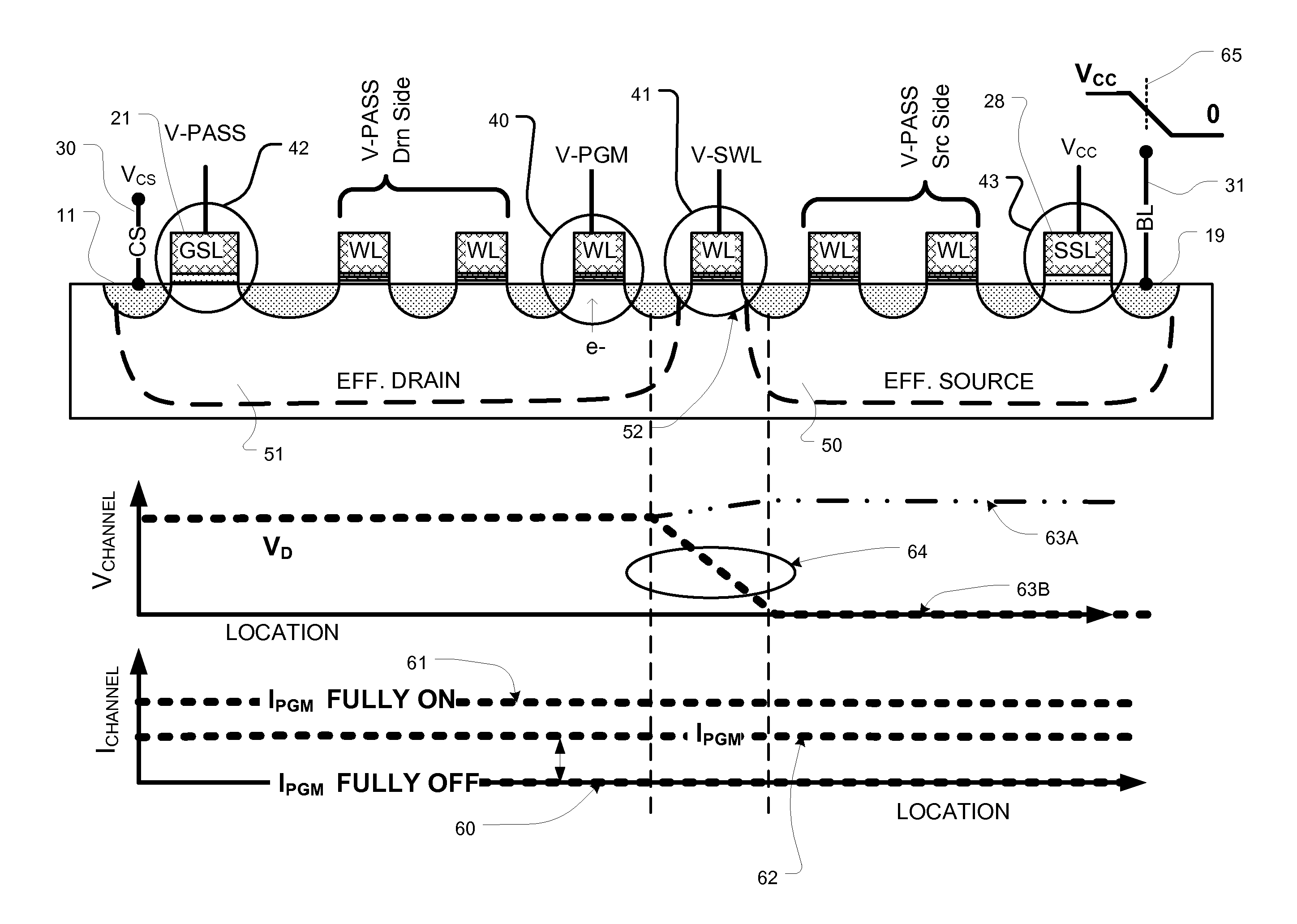
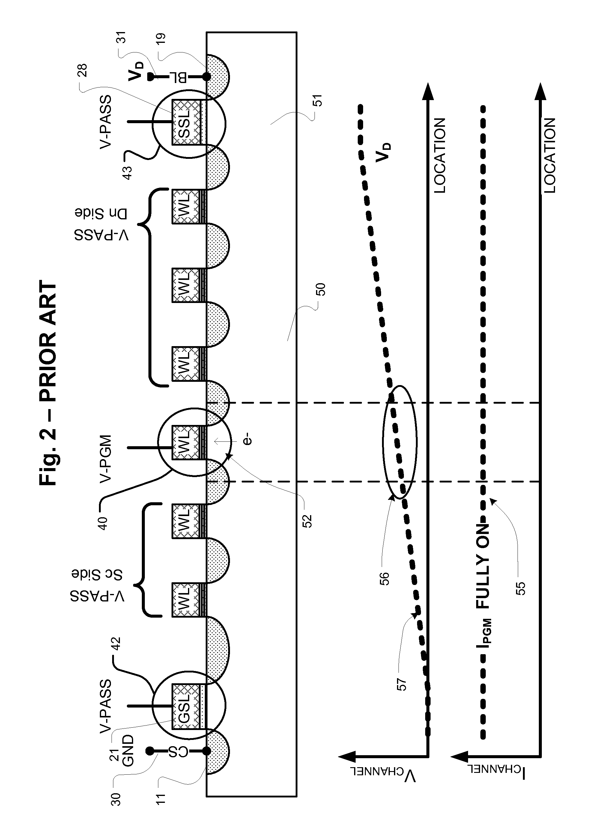
[0028]A detailed description of embodiments of the present invention is provided with reference to the FIGS. 1-10.
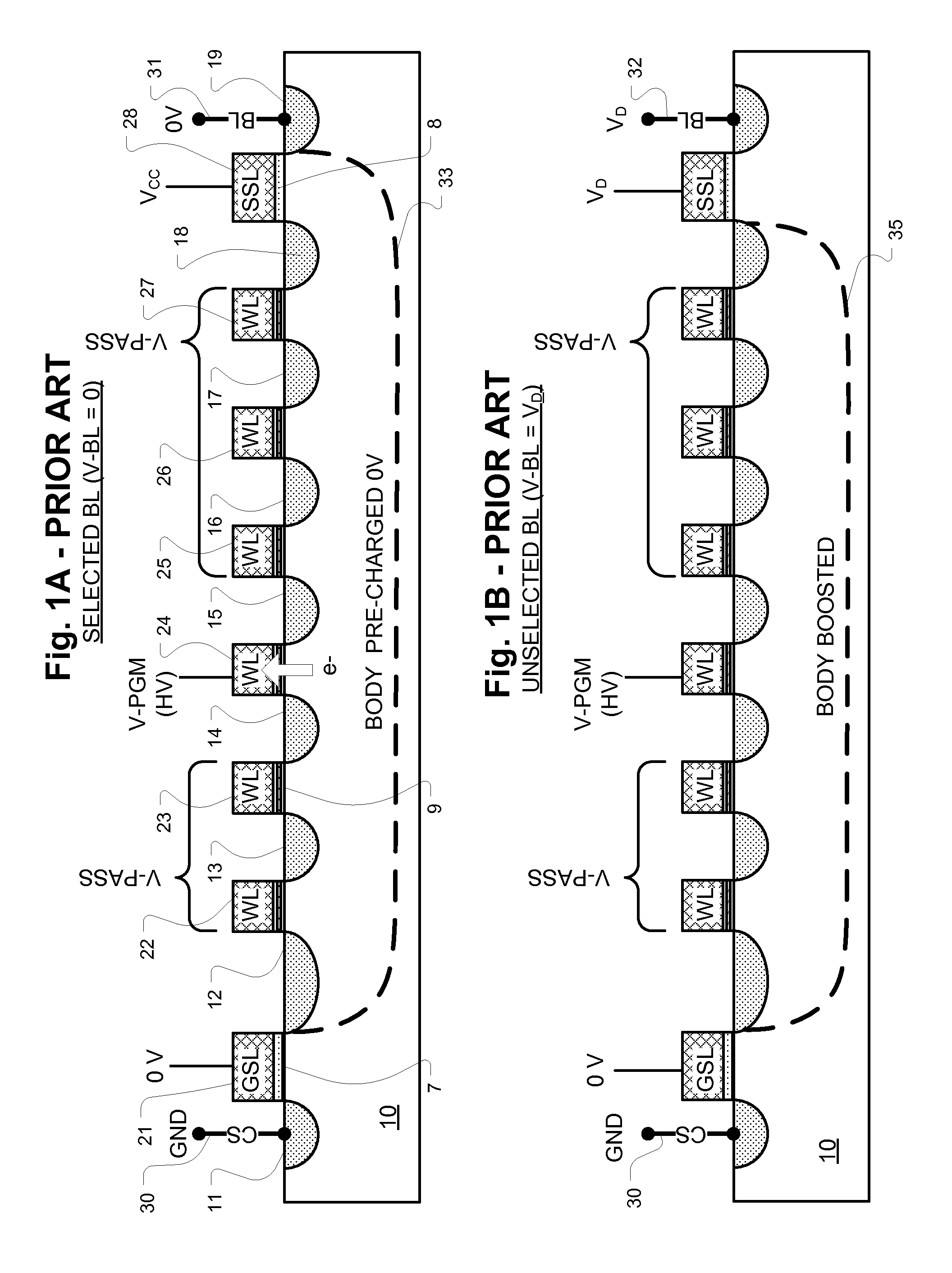
[0029]FIGS. 1A and 1B show in cross-section a plurality of dielectric charge trapping flash memory cells arranged in series to form a NAND string and biased for FN tunneling programming, as is typical in prior art NAND architecture flash memory. FIG. 1A shows the biasing for a NAND string that includes a target cell on a selected bit line, while FIG. 1B shows the biasing for a NAND string on an unselected bit line. One technology for implementation of NAND flash using bandgap engineered SONOS (BE-SONOS) charge trapping technology is described in U.S. Pat. No. 7,315,474 by Lue, which is incorporated by reference as if fully set forth herein. NAND strings can be implemented in a variety of configurations, including finFET technology, shallow trench isolation technology, vertical NAND technology and others. See, for an example vertical NAND structures, European Patent Appli...
PUM
 Abstract
Description
Claims
Application Information
 - R&D
- Intellectual Property
- Life Sciences
- Materials
- Tech Scout
- Unparalleled Data Quality
- Higher Quality Content
- 60% Fewer Hallucinations
Browse by: Latest US Patents, China's latest patents, Technical Efficacy Thesaurus, Application Domain, Technology Topic, Popular Technical Reports.
© 2025 PatSnap. All rights reserved.Legal|Privacy policy|Modern Slavery Act Transparency Statement|Sitemap|About US| Contact US: help@patsnap.com


