
Photolithographic apparatus

a technology of photolithography and apparatus, applied in the field of photolithographic apparatus, can solve the problems of less efficient reaction or cross-linking reaction, less light diffraction effect, and further degraded latent image of photoacid contrast, so as to improve the contrast of latent image and reduce the roughness of edge edges of photolithographic patterns

Active Publication Date: 2013-04-04
SEMICONDUCTOR MANUFACTURING INTERNATIONAL (BEIJING) CORP
View PDF4 Cites 2 Cited by
  • Summary
  • Abstract
  • Description
  • Claims
  • Application Information

AI Technical Summary

Benefits of technology

The patent is about a device called a photolithographic apparatus that uses a special photochemical called a photo-resist. The device has a light source that creates a chemical substance in the photo-resist using a specific wavelength of light. This chemical substance then reacts with another chemical substance produced by another light to reduce its concentration in the photo-resist. This reduces the likelihood of certain side effects like low contrast and rough edges in the final patterns created by the device.

Problems solved by technology

However, in practice, with the continuous shrinkage of the critical dimension for a semiconductor process, light diffraction effect becomes more severe, such that the part of the optical image that should have zero light intensity has a non-zero amount of light intensity.
As a result, the contrast of the latent image of the photoacid is further degraded.
However, the method is disadvantageous since it will make the removal reaction or the cross-linking reaction less efficient.
Moreover, the conventional method does not prevent the degradation of contrast of latent images caused by diffraction.

Method used


Image

  • Photolithographic apparatus
  • Photolithographic apparatus
  • Photolithographic apparatus

Examples


Embodiment Construction

[0064]Various exemplary embodiments of the present invention will now be described in detail with reference to the drawings. It should be noted that the relative arrangement of the components and steps, the numerical expressions, and numerical values set forth in these embodiments do not limit the scope of the present invention unless it is specifically stated otherwise.

[0065]It should be understood that, for the convenience of description, components in the figures are not necessarily drawn to scale.

[0066]The following description of at least one exemplary embodiment is merely illustrative in nature and is in no way intended to limit the invention, its application, or uses.

[0067]Techniques, methods and apparatus as known by one of ordinary skill in the relevant art may not be discussed in detail but are intended to be part of the specification where appropriate.

[0068]In the examples illustrated and discussed herein, any specific values should be interpreted to be illustrative and n...


PUM


Abstract

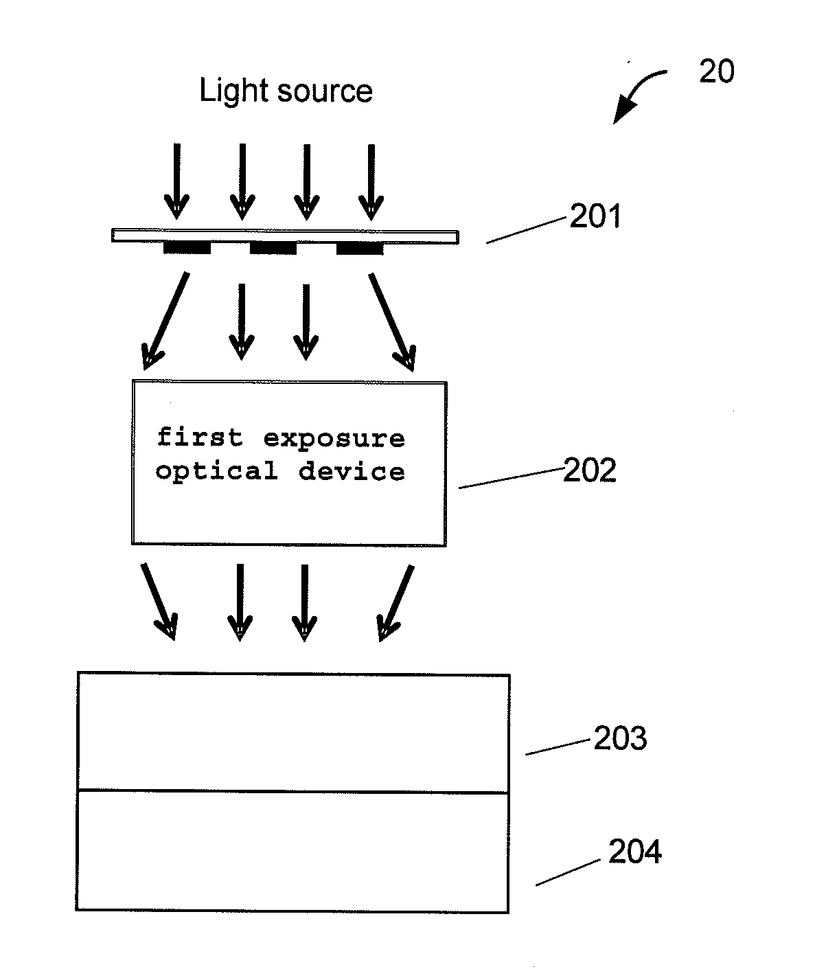
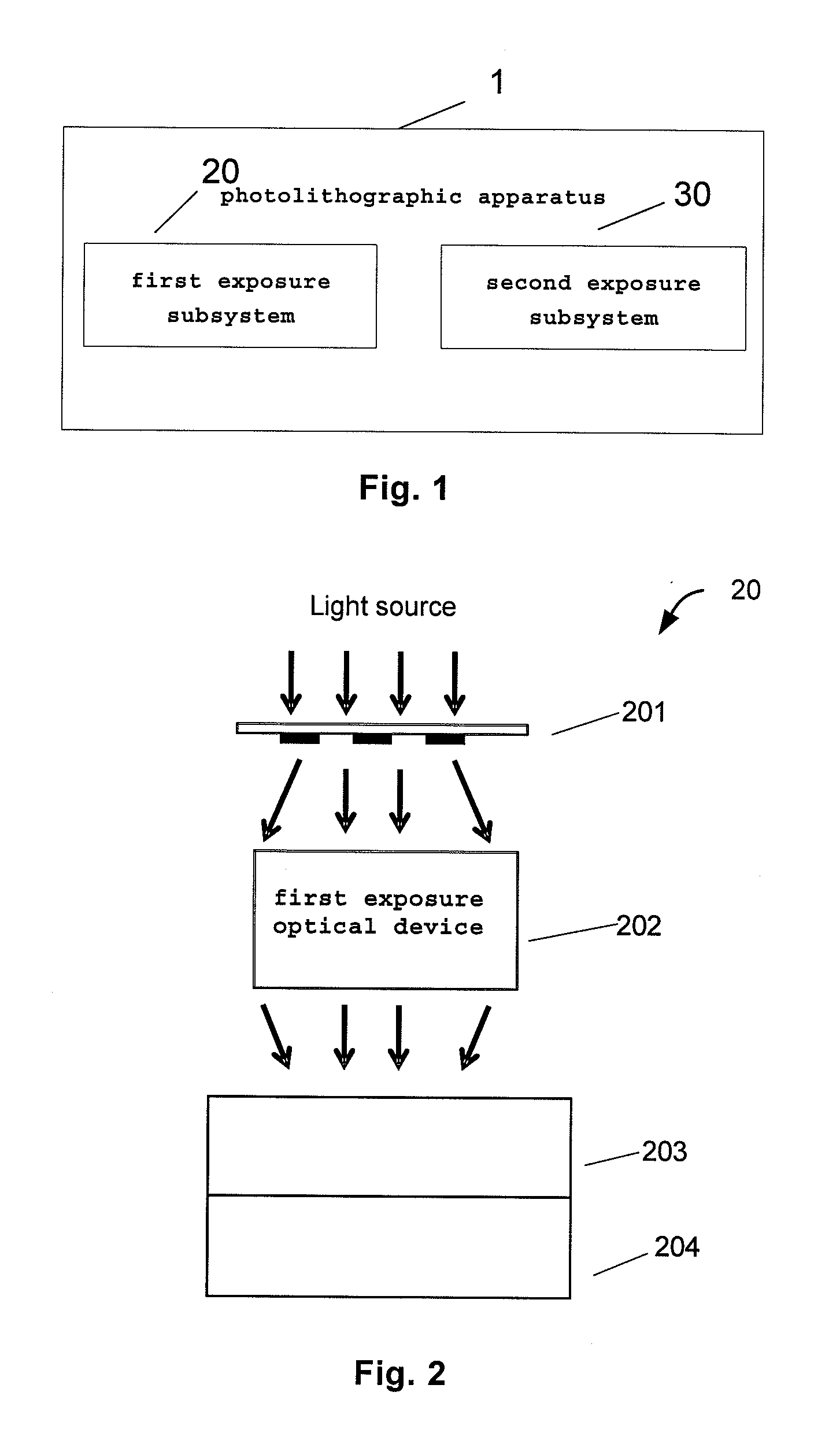
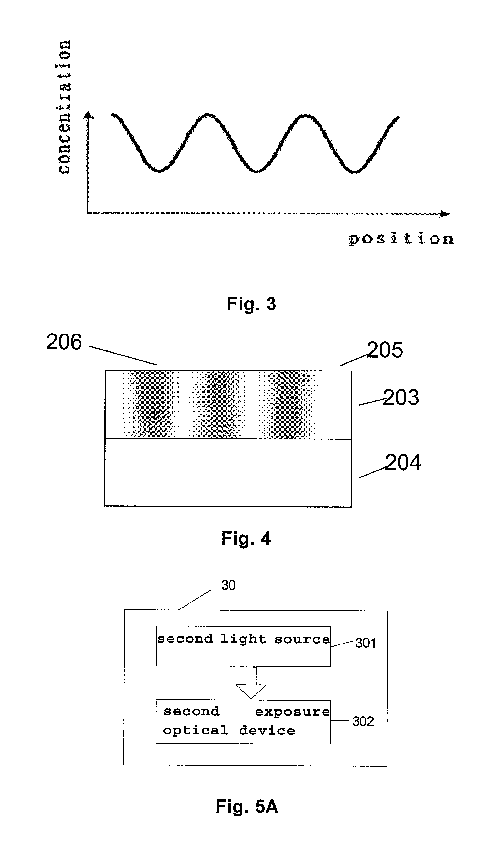
A photolithographic apparatus for use with a photo-resist comprises a first component that generates a first chemical substance and produces a chemical amplification action and a second component that generates a second chemical substance. The photolithographic apparatus comprises a first exposure subsystem for selectively illuminating a surface of the photo-resist using a light of a first wavelength band such that the first component generates the first chemical substance and a second exposure subsystem for uniformly illuminating the surface using a light of a second wavelength band such that the second component generates the second chemical substance. The second chemical substance reacts with the first chemical substance to reduce the mass concentration of the first chemical substance in the photo-resist and improves the contrast of a latent image of the first chemical substance formed in the photo-resist.

Description

CROSS-REFERENCES TO RELATED APPLICATIONS[0001]This application claims priority to Chinese Patent Application No. 201110295458.0, filed on Sep. 29, 2011 and entitled “Photolithographic Apparatus”, which is incorporated herein by reference in its entirety.[0002]This patent application is related to the following co-pending, commonly assigned patent applications, the disclosure of which are incorporated herein by reference in their entirety:[0003]1. “Photolithographic Method” by Qiang Wu and Yao Xu, Attorney Docket No. 87720-030500US-826645, filed concurrently herewith.[0004]2. “Photo-resist and Method of Photolithography” by Qiang Wu and Yiming Gu, Attorney Docket No. 87720-030600US-826644, filed concurrently herewith.BACKGROUND OF THE INVENTION[0005]1. Field of the Invention[0006]The present invention relates generally to a photolithographic apparatus, and more specifically, to a photolithographic apparatus for a photo-resist that contains a photoacid generator and a photobase genera...

Claims


Application Information

Patent Timeline
Patent Type & Authority Applications(United States)
IPC IPC(8): G03B27/32
CPCG03F7/70466G03F7/203G03F7/70575
Inventor WU, QIANGGU, YIMING
Owner SEMICONDUCTOR MANUFACTURING INTERNATIONAL (BEIJING) CORP
Learn More