Semiconductor device having stacked layers

Inactive Publication Date: 2013-03-21
LONGITUDE LICENSING LTD
View PDF4 Cites 208 Cited by
  • Summary
  • Abstract
  • Description
  • Claims
  • Application Information

AI Technical Summary

Benefits of technology

The semiconductor device described in this patent has a structure that allows for faster and more efficient memory reading. It includes a first substrate with memory cells and bit lines, a second substrate with a sense amplifier, and a third substrate with a selection circuit. The first transistor is slower than the second transistor, and the second transistor is faster than the third transistor. This arrangement ensures quicker and more reliable memory reading.

Problems solved by technology

When applying the above conventional techniques to a memory, it is difficult to ensure a high-speed operation.
Therefore, on-current of the transistor becomes small and the high-speed operation is hindered.
Further, in the technique disclosed in the above Non-Patent References 7 to 9, a process needs to be added when manufacturing a semiconductor memory, in which a monocrystalline silicon wafer having an oxide film and ion-implanted with hydrogen is formed into a thin film and the film, is stacked, thereby increasing manufacturing cost.

Method used


Image

  • Semiconductor device having stacked layers
  • Semiconductor device having stacked layers
  • Semiconductor device having stacked layers

Examples


Embodiment Construction

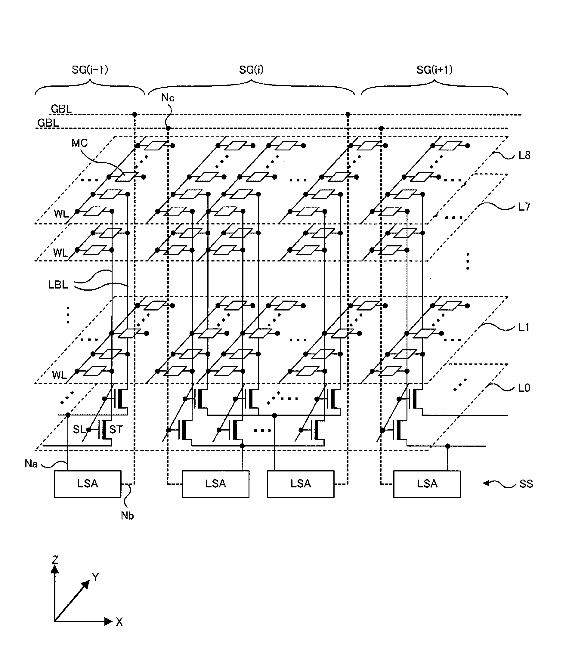
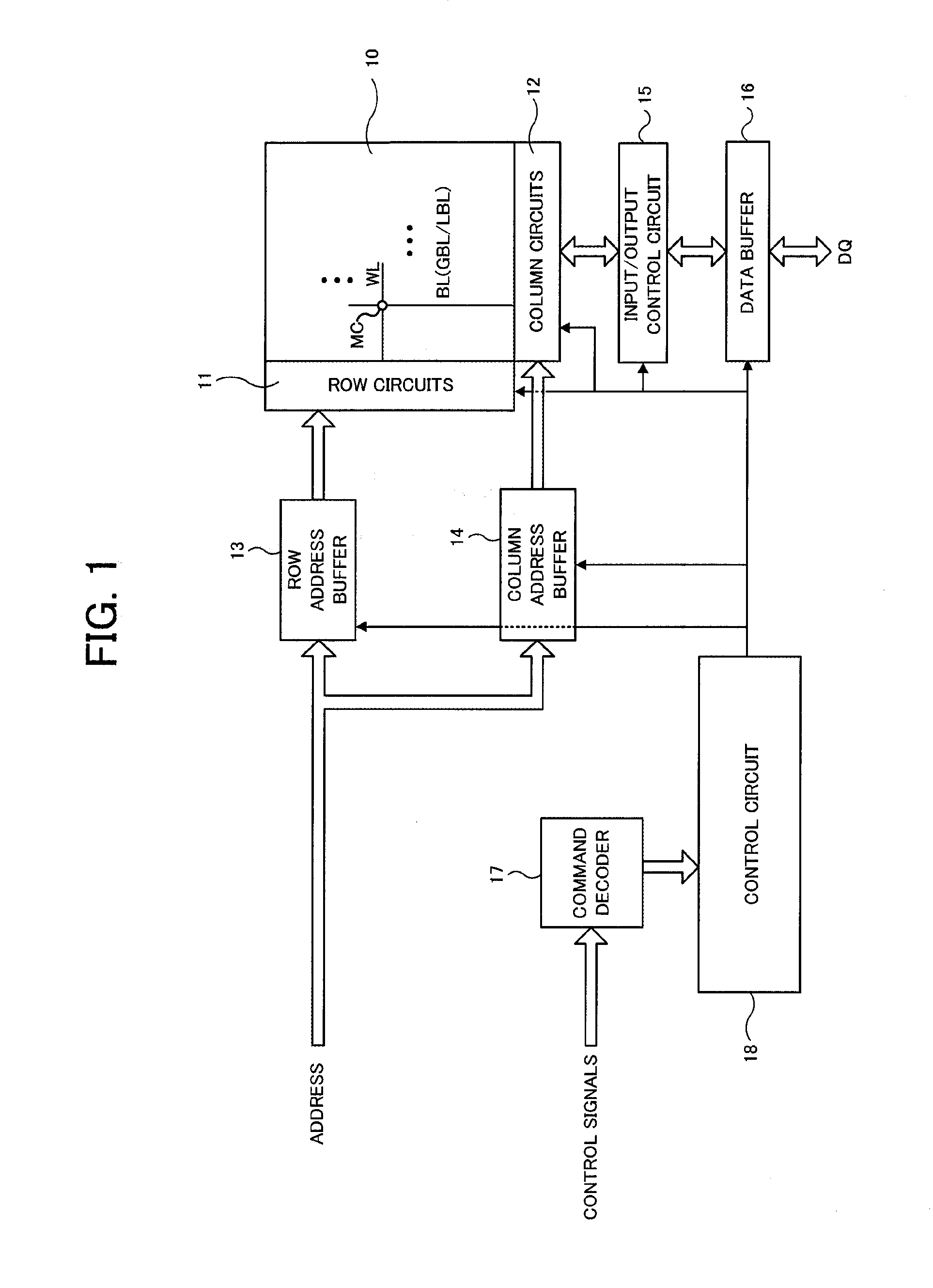
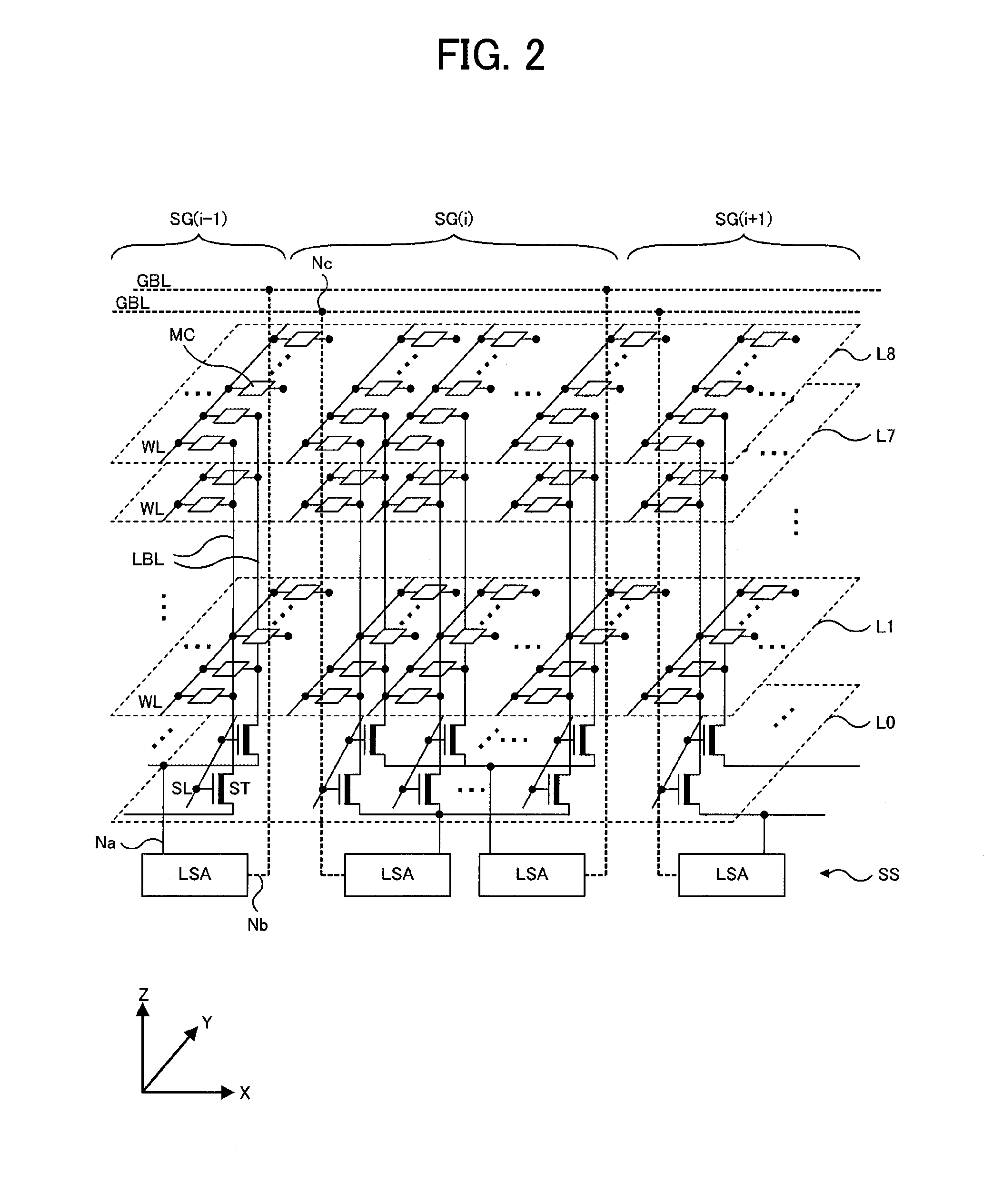
[0036]In the following, preferred embodiments of the invention will be described in detail with reference to accompanying drawings. FIG. 1 is a block diagram showing an entire configuration of a semiconductor device of an embodiment, which shows, for example, a configuration example of a volatile DRAM (Dynamic Random Access Memory). In the semiconductor device shown in FIG. 1, there are provided a memory cell array 10 including a plurality of memory cells MC each storing data, and row circuits 11 and column circuits 12 that are attached to the memory cell array 10. The row circuits 11 include circuits provided corresponding to a plurality of word lines WL, and the column circuits 12 include circuits provided corresponding to a plurality of bit lines BL. It is preferred that the memory cell array 10 has a hierarchical bit line structure, and in this embodiment, the bit lines BL are hierarchized into local bit lines LBL of a lower hierarchy and global bit lines GEL of an upper hierarc...


PUM


Abstract

A semiconductor device is disclosed in which there are provided a first substrate including memory cells and at least one bit line electrically coupled to the memory cells, and a second substrate including a sense amplifier. Each of the memory cells includes a first transistor, and the sense amplifier includes a second transistor. The second substrate is stacked with the first substrate such that the sense amplifier amplifies data transferred through the bit line from a selected one of the memory cells. The first transistor is lower in carrier mobility than the second transistor.

Description

BACKGROUND OF THE INVENTION[0001]1. Field of the Invention[0002]The present invention relates to a semiconductor device in which TFTs are formed in layers stacked on a substrate.[0003]2. Description of Related Art[0004]Semiconductor devices of recent years have employed a stacked-type memory cell array having a multilayer structure on a substrate in order to deal with an increase in capacity and a reduction in size. Attention has been focused on a technique for forming a transistor in such a memory cell array, in which semiconductor material capable of being stacked in a low temperature process such as polysilicon or oxide semiconductor is used to form a channel. For example, a structure has been proposed which includes a transistor in which the polysilicon is used as the channel in a stacked-type NAND flush memory (for example, see Non-Patent References 1 to 6). Further, for example, a structure has been proposed in which a stacked-type DRAM, NAND flush memory, or ReRAM / PCRAM is fo...

Claims


Application Information

Patent Timeline
IPC IPC(8): G11C5/02G11C7/06
CPCG11C7/18G11C11/4097G11C11/4076H10B63/845H10B63/30H10N70/823H10N70/20
Inventor KAJIGAYA, KAZUHIKO
Owner LONGITUDE LICENSING LTD
Why Eureka
Try Eureka