Semiconductor device and solid state relay using same
a solid-state relay and semiconductor technology, applied in the direction of semiconductor/solid-state device details, electronic switching, pulse technique, etc., can solve the problems of increasing crystal defects, increasing crystal defects, and increasing on-resistance, so as to suppress the increase of on-resistance of sic-mosfets, prevent the increase of crystal defects of epitaxial growth layers, and high repeat number of switching
- Summary
- Abstract
- Description
- Claims
- Application Information
AI Technical Summary
Benefits of technology
Problems solved by technology
Method used
Image

Examples
first embodiment
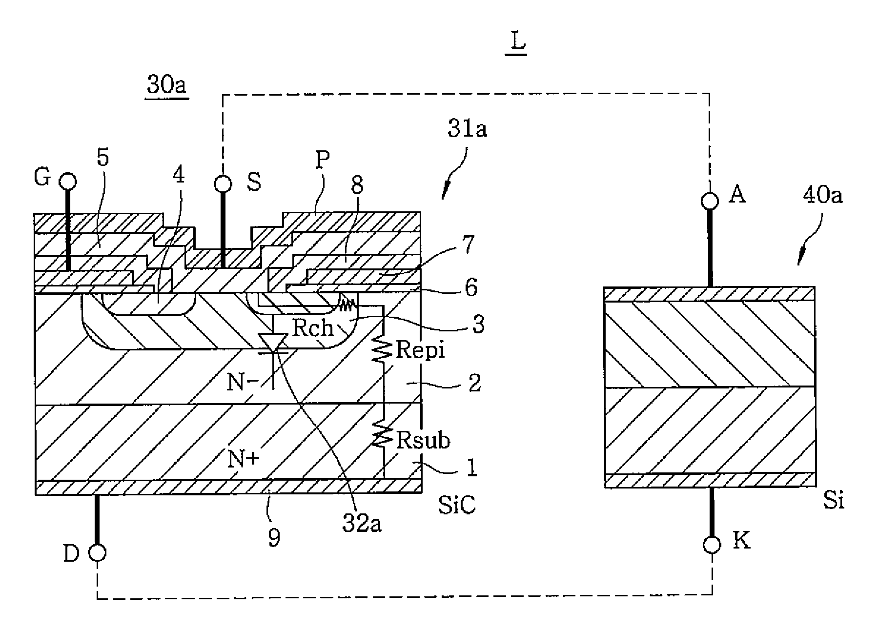
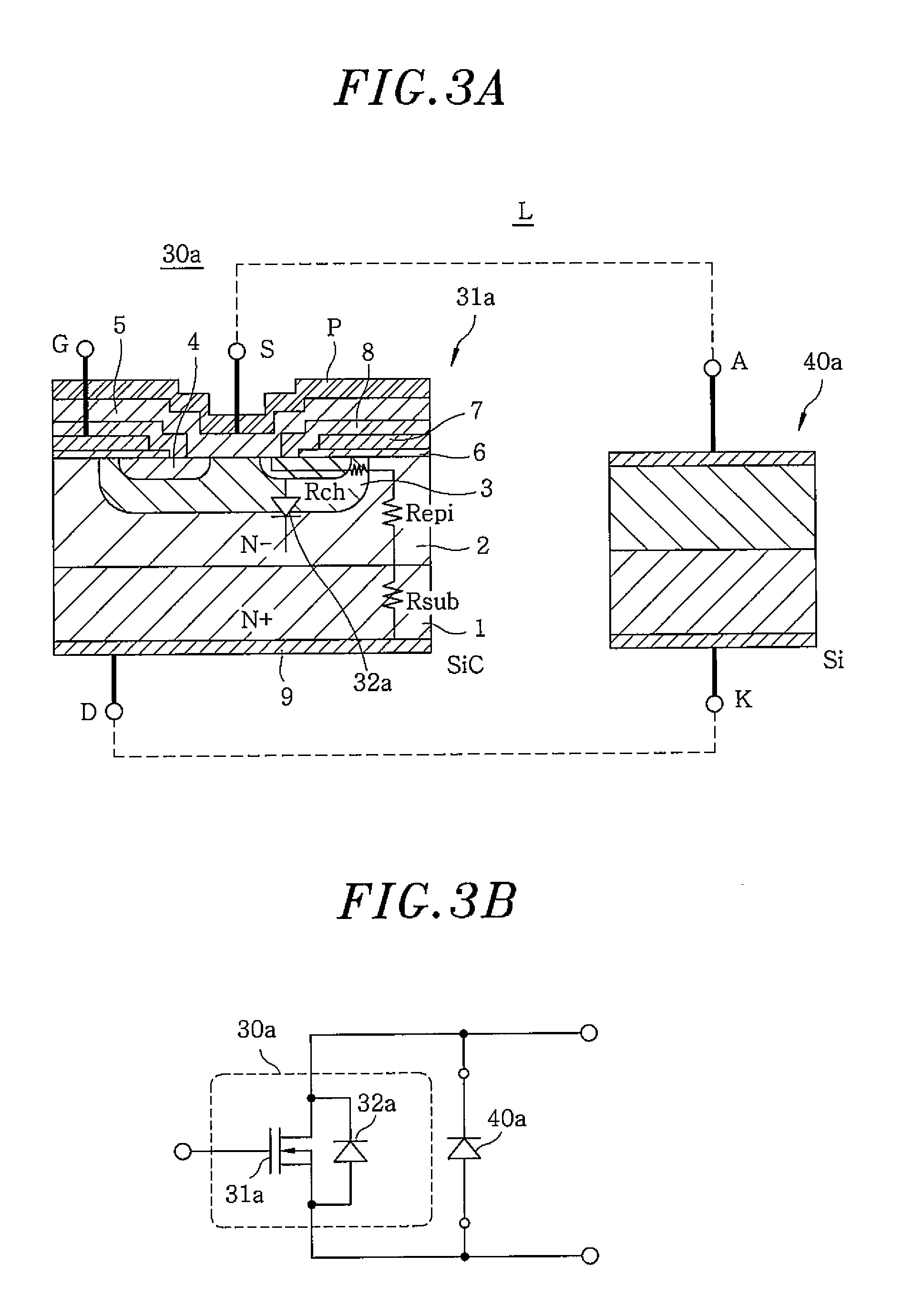
[0036]A solid state relay in accordance with a first embodiment of the present invention features an output element formed of a compound semiconductor element, e.g., a SiC-MOSFET to which a silicon diode is externally connected, the silicon diode being employed as a protection element for the output element. A semiconductor device of the present embodiment includes at least one unipolar compound semiconductor element serving as the output element; and bypass semiconductor elements serving as the protection element, the bypass semiconductor elements being externally connected in parallel to the compound semiconductor elements, respectively. At this time, the turn-on voltage of the bypass semiconductor elements is smaller than the turn-on voltage of the compound semiconductor elements in the direction from the source to the drain.
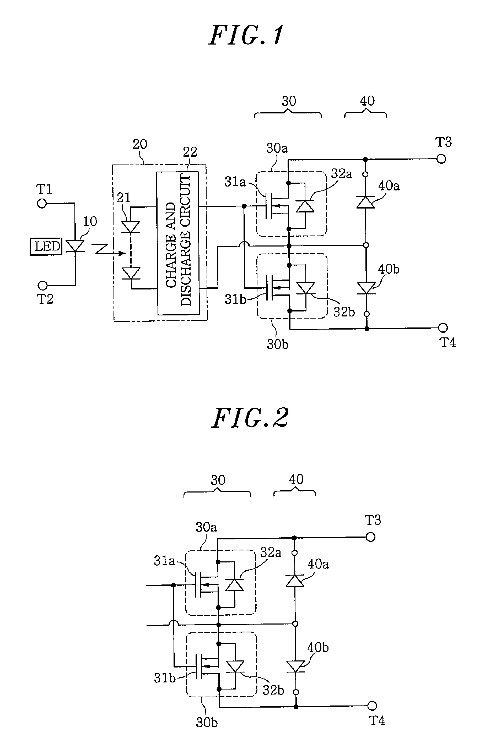
[0037]The solid state relay of the present embodiment includes a light emitting element which emits lights in response to an input signal; a photodiode array...
second embodiment
[0059]As shown in FIG. 7, in a semiconductor device in accordance with a second embodiment, a bypass semiconductor element, serving as a protection element, is formed of a Si-MOSFET 51 in such a way that a drain and a source of the Si-MOSFET 51 are respectively connected to the drain and the source of the SiC-MOSFET 31.
[0060]Comparing a body diode 52 provided with the Si-MOSFET 51 and the SiC-pn (body) diode 32 connected in parallel in the direction from the source to the drain in the above configuration, a forward-direction drop voltage Vf (about 0.6 V) of the body diode 52 is smaller than a forward-direction drop voltage Vf (about 3 V) of a SiC-pn (body) diode 32.
[0061]Accordingly, when a positive voltage and a negative voltage are respectively applied to the source and the drain, a current, which is scheduled to flow through the SiC-pn (body) diode 32 if no body diode 52 is provided, will bypass it to the body diode 52 of the Si-MOSFET 51.
[0062]As a result, it is possible to prev...
third embodiment
[0063]As shown in FIG. 8, in a semiconductor device in accordance with a third embodiment, a bypass semiconductor element serving as a protection element is a SiC-Schottky diode 60 in such a way that a cathode and an anode of the SiC-Schottky diode 60 are respectively connected to the drain and the source of the SiC-MOSFET 31.
[0064]FIG. 9 is a graph showing the result of measuring the relationship between a voltage and a conduction current in the SiC-Schottky diode 60 and the SiC-pn (body) diode 32 that are connected in parallel in the direction from the source to the drain. As shown in FIG. 9, when the conduction current is equal to or lower than a crossover current Icross, a forward-direction drop voltage Vf (curve “b”) of the SiC-Schottky diode 60 is smaller than a forward-direction drop voltage Vf (curve “a”) of a SiC-pn (body) diode 32. Accordingly, when a positive voltage and a negative voltage are respectively applied to the source and the drain, a current, which is scheduled...
PUM
 Abstract
Description
Claims
Application Information
 - R&D
- Intellectual Property
- Life Sciences
- Materials
- Tech Scout
- Unparalleled Data Quality
- Higher Quality Content
- 60% Fewer Hallucinations
Browse by: Latest US Patents, China's latest patents, Technical Efficacy Thesaurus, Application Domain, Technology Topic, Popular Technical Reports.
© 2025 PatSnap. All rights reserved.Legal|Privacy policy|Modern Slavery Act Transparency Statement|Sitemap|About US| Contact US: help@patsnap.com