Semiconductor device and manufacturing method thereof

Inactive Publication Date: 2013-02-28
SEMICONDUCTOR MANUFACTURING INTERNATIONAL (BEIJING) CORP
View PDF9 Cites 1 Cited by
  • Summary
  • Abstract
  • Description
  • Claims
  • Application Information

AI Technical Summary

Benefits of technology

This patent aims to provide a method for manufacturing semiconductor devices that protects the metal gate from oxidation during the deposition of an interlayer dielectric and etching of contact holes. The method includes the use of an interface layer that is easy to etch and can reduce contact resistance. The resulting semiconductor devices have improved contact CD, consistent contact resistance, a good process window for dielectric interlayer deposition, reduced voiding, and reduced leakage from the top of the gate.

Problems solved by technology

However, with the shrinkage of contact critical dimensions, the manufacturing process encounters challenges and open contact risk is increased as well.
For example, due to the shrinkage of contact critical dimensions, a relatively thick resist may cause a contact hole (or, opening) etching to stop.
Moreover, it is difficult to shrink the contact CD to a desired target value.
The metal oxide layer thus formed may be dense and is difficult to etch, particularly for aluminium oxide.

Method used


Image

  • Semiconductor device and manufacturing method thereof
  • Semiconductor device and manufacturing method thereof
  • Semiconductor device and manufacturing method thereof

Examples


Embodiment Construction

[0041]The embodiments of the present invention will be described below in conjunction with the drawings.

[0042]FIGS. 1-7 show steps in a method of manufacturing a semiconductor device according to an embodiment of the present invention.

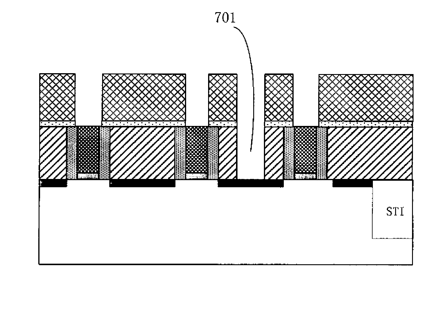
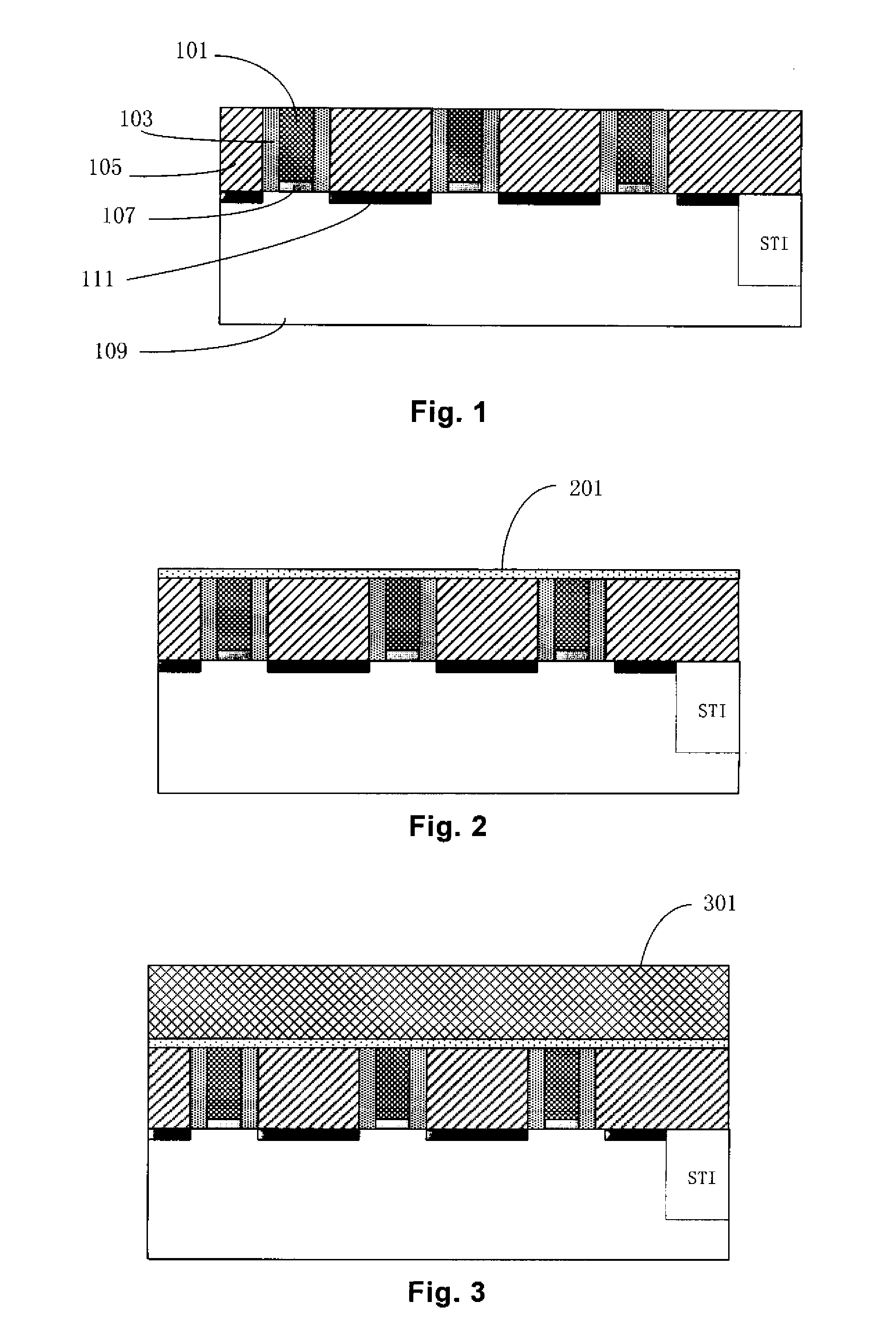
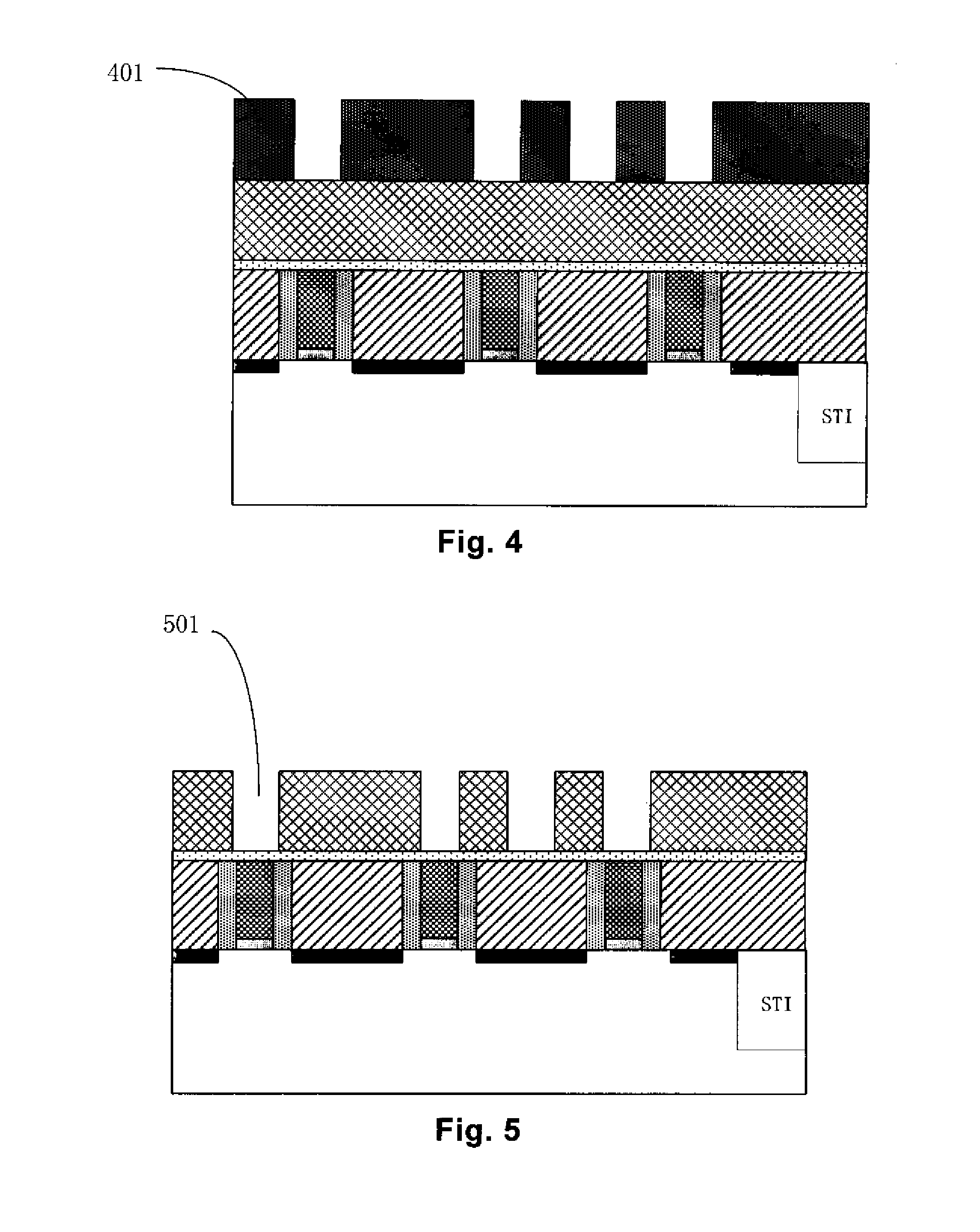
[0043]As shown in FIG. 1, a substrate 109 which includes shallow trench isolation (STI), for a semiconductor device is provided with a gate structure and a first dielectric interlayer 105 formed on the substrate 109. The gate structure comprises a metal gate 101. An upper surface of the first dielectric interlayer 105 is substantially flush with an upper surface of the gate 101.

[0044]The substrate is typically a mono-crystalline silicon substrate. However, the present invention should not be limited thereto. According to different applications, the substrate can be a semiconductor-on-semiconductor (SOI) substrate, a poly-silicon substrate, a compound semiconductor substrate, an insulating substrate (e.g. a glass substrate) having a semiconductor materi...


PUM


Abstract

A semiconductor device and a manufacturing method thereof is provided. The method comprises: providing a substrate for the semiconductor device with a gate structure and a first dielectric interlayer being formed thereon, said gate structure comprising a metal gate and an upper surface of said first dielectric interlayer being substantially flush with an upper surface of said gate; forming an interface layer to cover at least the upper surface of said gate such that the upper surface of said gate is protected from being oxidized; and forming a second dielectric interlayer on said interface layer.

Description

CROSS-REFERENCE TO RELATED APPLICATIONS[0001]This application claims priority to Chinese Patent Application No. 201110246794.6, filed on Aug. 26, 2011 and entitled “Semiconductor Device and Manufacturing Method thereof”, which is incorporated in its entirety herein by reference.FIELD OF THE INVENTION[0002]The present invention relates to the field of semiconductor fabrication techniques, and more specifically, relates to semiconductor devices and manufacturing methods therefor.DESCRIPTION OF THE RELATED ART[0003]As known by those of ordinary skill in the art, there is a gate-last approach and a gate-first approach for manufacturing a semiconductor device such as a field-effect transistor.[0004]In the gate-last approach, referring to Fig. 8, a dielectric layer 807 and a dummy gate are formed on a substrate 809, preferably, a lightly doped region (LDD) implantation of the substrate 809 is carried out, and then one or more spacers 803 are formed; after the formation of such a dummy gat...

Claims


Application Information

Patent Timeline
IPC IPC(8): H01L29/78H01L21/336
CPCH01L29/78H01L21/76801H01L29/66575H01L23/564H01L21/76816H01L2924/0002H01L2924/00
Inventor WANG, XINPENGHUANG, YICHANG, SHIH-MOU
Owner SEMICONDUCTOR MANUFACTURING INTERNATIONAL (BEIJING) CORP
Why Eureka
Try Eureka