Method of fabricating circuit board

a circuit board and fabrication method technology, applied in the direction of printed circuit manufacturing, superimposed coating process, coating, etc., can solve the problems of insufficient polishing, short circuit, and inability to flow specified current in the wiring, so as to suppress the occurrence of defocus, reduce roll-off, and suppress the effect of lack of cutting or excessive cutting of the conductor layer

Inactive Publication Date: 2013-02-07
NGK SPARK PLUG CO LTD
View PDF6 Cites 5 Cited by
  • Summary
  • Abstract
  • Description
  • Claims
  • Application Information

AI Technical Summary

Benefits of technology

[0013]In the method of fabricating a circuit board according to the first aspect of the present invention, the conductor layer to serve as the wiring layer is formed such that at least a portion of the conductor layer is embedded in the wiring trench formed in the insulation layer, and a surface of the conductor layer formed is cut with a cutting tool. Accordingly, when the surface of the conductor layer is cut, a configuration of the cut surface of the conductor layer can be less influenced by a configuration (for instance, concave portions and convex portions) of the insulation layer and the conductor layer, so that lack of cutting or excessive cutting of the conductor layer can be suppressed. Further, since the surface of the conductor layer is treated by the cutting work, it is possible to reduce roll-off in a metal material of the conductor layer which will occur during the polishing work. Further, since a configuration of the cut surface of the conductor layer can be less influenced by a configuration (for instance, concave portions and convex portions) of the insulation layer and the conductor layer, the cut surface of the conductor layer can be flat in shape. Therefore, even in a case where a laminated structure is formed by a plurality of insulation layers and a plurality of wiring layers, a surface of the circuit board can be formed into a flat shape to thereby suppress occurrence of defocus upon being exposed to light.
[0014]Further, a diamond bite can be used as the cutting tool. The diamond bite has a remarkably high wear resistance, and therefore, the diamond bite can be used for a long period of time. Further, a surface roughness of the conductor layer which is obtained when the cutting work is finished is low, thereby reducing concave portions and convex portions which are generated on the surface of the wiring layer. As a result, it is possible to reduce electric noise that is generated in the wiring layer. Furthermore, the diamond bite has a high hardness, thereby conducting the cutting work at high speed and enhancing productivity.
[0015]Further, in a further aspect of the present invention, there is provided the method of fabricating a circuit board, wherein in the third step, the surface of the conductor layer as well as the surface of the insulation layer are cut to form a roughened surface on the insulation layer. By forming the roughened surface on the insulation layer, adhesion of the insulation layer to the insulation layer to be laminated on the cut surface (i.e., the roughened surface) of the insulation layer can be enhanced. Further, since the surface of the insulation layer is cut, it is not necessary to remove the wiring material adhered to the surface of the insulation layer when the wiring layer is formed. As a result, the fabricating process of the circuit board can be simplified.
[0016]Further, in a still further aspect of the present invention, there is provided the method of fabricating a circuit board, wherein in the third step, the cutting operation is repeatedly carried out plural times in a plurality of stages. By carrying out the cutting operation plural times in the plurality of stages, it is possible to perform the cutting work with a high accuracy. Further, even in a case where the conductor layer has a large thickness, the conductor layer can be well subjected to cutting.
[0017]Furthermore, in a still further aspect of the present invention, there is provided the method of fabricating a circuit board, wherein the second step includes a step of forming a first conductor layer in the wiring trench by electroless plating, and a step of forming a second conductor layer on the first conductor layer by electroplating. By previously subjecting the insulation layer to electroless plating, the conductive layer can be formed by electroplating with a high film forming speed. As a result, productivity of the circuit board can be enhanced.
[0018]The method of fabricating a circuit board according to the present invention can attain an effect of suppressing excessive cutting and lack of cutting of a conductor layer that serves as a wiring layer.

Problems solved by technology

Therefore, there is generated a local area of the conductor layer which is excessively polished, or there is contrarily generated is polished in an insufficient degree.
Further, even in a case where a surplus of the conductor layer is removed by another process except for CMP, for instance, wet etching, a thickness of the conductor layer formed by plating also tends to become non-uniform to thereby cause the same problems as described above.
In a case where a local area of the conductor layer is excessively polished, a thickness of the wiring formed in the local area becomes smaller so that there will occur a problem that specified current cannot be flowed in the wiring.
On the other hand, in a case where a region of the conductor layer is polished in an insufficient degree, there will occur a problem that a short circuit is caused between adjacent portions of the wiring in the region of the conductor layer due to lack of polishing.

Method used


Image

  • Method of fabricating circuit board
  • Method of fabricating circuit board
  • Method of fabricating circuit board

Examples


example

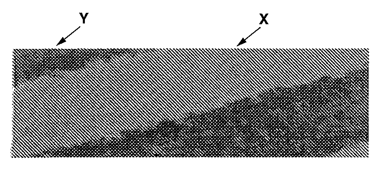
[0057]Next, an example of the method of fabricating the circuit board 1 of the present invention is explained. In the example, in accordance with the fabricating method as described above, a test piece was prepared by forming a copper plating layer embedded in a wiring trench in a resin insulation layer, and then subjecting the copper plating layer to cutting with a diamond bite. A cut surface of the thus obtained test piece was observed by a SEM.

[0058](Preparation of Test Piece)

An insulating film made of a resin material containing an epoxy resin as a main component was laminated on a surface of a plate-like resin substrate as a core substrate to thereby form a laminate. Thus obtained laminate was pressed under heating using a vacuum compression-bonding hot press so that the insulating resin film was compression-bonded to the core substrate while being heat-cured. Next, the laminate was subjected to laser irradiation with a laser processing machine, thereby forming a wiring trench ...


PUM

PropertyMeasurementUnit
sizeaaaaaaaaaa
depthaaaaaaaaaa
insulatingaaaaaaaaaa

Abstract

A method of fabricating a circuit board including at least one insulation layer and at least one wiring layer, the method including a first step of forming a wiring trench in a surface of the insulation layer, a second step of forming a conductor layer serving as the wiring layer in the wiring trench such that at least a portion of the conductor layer is embedded in the wiring trench, and a third step of cutting a surface of the conductor layer with a cutting tool to form the wiring layer.

Description

BACKGROUND OF THE INVENTION[0001]The present invention relates to a method of fabricating a circuit board, and particularly, relates to a method of fabricating a circuit board in which a wiring trench is formed in an insulation layer and a conductor layer is formed in the wiring trench.[0002]A method of fabricating a circuit board, for instance, a semi-additive process has been conventionally known. In the semi-additive process, a laminate formed by laminating an insulating film made of a resin material which contains an epoxy resin as a main component on a core substrate is pressed under heating using a vacuum compression-bonding hot press so that the insulating resin film is bonded to the core substrate while being heat-cured. Subsequently, via holes are formed in the insulating resin film by laser irradiation or the like. Then, an electroless plating layer is formed on the insulating resin film so as to cover an inner peripheral wall thereof which defines the respective via holes...

Claims


Application Information

Patent Timeline
Patent Type & Authority Applications(United States)
IPC IPC(8): C23C28/00
CPCC25D3/38C25D5/48H05K2203/025H05K3/465H05K3/045H05K3/46
Inventor MURAMATSU, MASAKIIZUMI, MASAONISHIO, KENJISATO, HIRONORI
Owner NGK SPARK PLUG CO LTD
Why Eureka
Try Eureka