A high-efficiency, low-roll-off phosphorescent organic light-emitting diode

A technology of light-emitting diodes and organic light-emitting layers, applied in semiconductor devices, electrical components, circuits, etc., can solve the problems of increasing phosphorescent OLED heterojunction interface, complex preparation process, high driving voltage, etc., and achieve balanced electron and hole distribution. , the effect of wide carrier recombination region and high device efficiency

Active Publication Date: 2019-10-29
TAIYUAN UNIV OF TECH
View PDF3 Cites 0 Cited by
  • Summary
  • Abstract
  • Description
  • Claims
  • Application Information

AI Technical Summary

Problems solved by technology

For example, the D-EML structure phosphorescent OLED has a very narrow carrier recombination region, and the efficiency roll-off at high voltage is still serious; the MH-EML structure phosphorescent OLED also inevitably makes the carriers at the two interfaces of the light-emitting layer Aggregation occurs, causing efficiency roll-off; G-EML structure phosphorescent OLED requires continuous change of the doping concentration of the luminescent material in the host material during the preparation process, which makes the preparation process of the device very complicated and the repeatability is very low; QW-EML Structured phosphorescent OLED introduces a multi-layer spacer material with a large difference in HOMO and LOMO energy levels between the host material and the host material in the light-emitting layer. The introduction of these spacer materials greatly increases the heterojunction interface in the phosphorescent OLED, resulting in a device with high drive voltage and low efficiency

Method used


Image

  • A high-efficiency, low-roll-off phosphorescent organic light-emitting diode
  • A high-efficiency, low-roll-off phosphorescent organic light-emitting diode
  • A high-efficiency, low-roll-off phosphorescent organic light-emitting diode

Examples


preparation example Construction

[0058] During the preparation process of the device, the evaporation rate of the material and the thickness of the organic and inorganic film layers are monitored and controlled by a quartz crystal frequency meter connected outside the vacuum chamber. Among them, organic materials, MoO 3 The evaporation rates of LiF, LiF, and Al are about 1Å / s, 0.3Å / s, 0.1Å / s, and 3Å / s, respectively. The overlapping part of the ITO glass and the aluminum cathode is used as the effective light-emitting layer of the device, and the effective light-emitting area is 3mm×3mm.

[0059] The performance test method of the OLED device involved in the embodiment of the present invention is as follows.

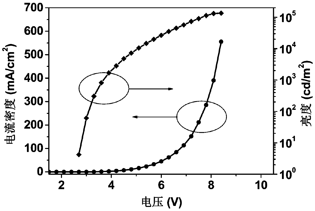
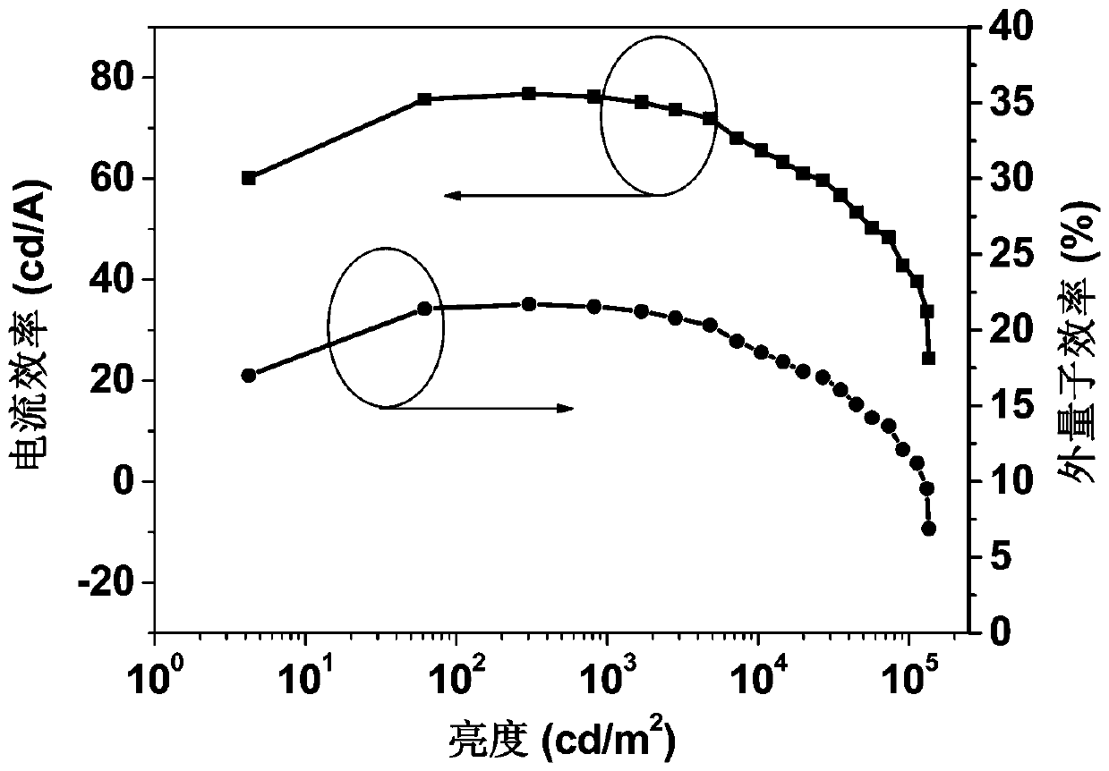
[0060] Take out the prepared white OLED device from the vacuum cavity, and measure the current density, luminance, current efficiency and power efficiency of the device by using the computer integrated control ST-900M photometer and Keithley 2400 digital source meter; use computer integrated control Th...

Embodiment 1

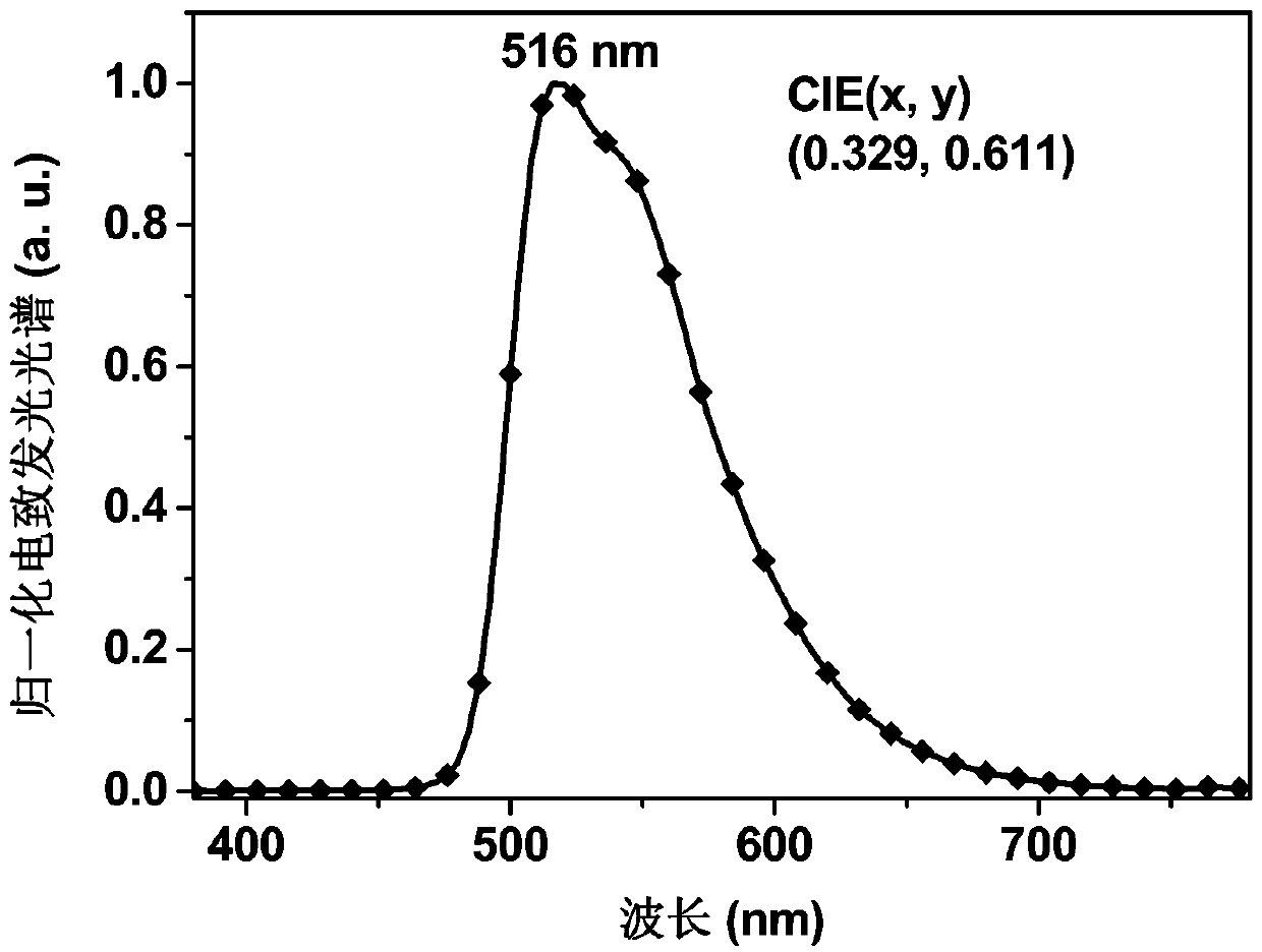
[0064] A green phosphorescent OLED device was prepared according to the above specific embodiments. The specific device structure is ITO / MoO 3 (3nm) / TAPC (40 nm) / TCTA: 7wt%Ir(ppy) 3 (5 nm) / TCTA: Bepp 2 (1:1): 7wt%Ir(ppy) 3 (10 nm) / Bepp 2 : 7wt%Ir(ppy) 3 (5 nm) / TmPyPB (50 nm) / LiF (1 nm) / Al (100 nm).

[0065] In the above green phosphorescent OLED device, 3 nm thick MoO 3 Thin layer is HIL, 40nm thick TAPC layer is HTL, 5nm thick TCTA: 7wt%Ir(ppy) 3 Layer as first EML, 10nm thick TCTA: Bepp 2 (1:1): 7wt%Ir(ppy) 3 The layer is the second EML, 5nm thick Bepp 2 : 7wt%Ir(ppy) 3 The layer is the third EML, the 50nm thick TmPyPB layer is the ETL, the 1nm thick LiF is the EIL, the ITO is the anode, and the 100nm thick Al film is the cathode.

[0066] figure 1 The electroluminescence spectrum of the device of this example at a voltage of 5V is given. It can be seen that the device emits very good green light, and there is only one emission peak in the electroluminesce...

Embodiment 2

[0070] In order to further prove the feasibility of the high-efficiency, low-roll-off phosphorescent organic light-emitting diode structure proposed by the present invention, this example keeps the device structure, functional materials and thin layer thickness of Example 1 unchanged, and uses the yellow phosphorescent material Ir(bT) 2 (acac) instead of green phosphorescent material Ir(ppy) 3 Doped in the host material, the yellow phosphorescent OLED device is prepared. The specific device structure is ITO / MoO 3 (3 nm) / TAPC (40 nm) / TCTA: 6wt% Ir(bT) 2 (acac) (5 nm) / TCTA:Bepp 2 (1:1): 6wt% Ir(bT) 2 (acac) (10 nm) / Bepp 2 : 6wt% Ir(bT) 2 (acac) (5 nm) / TmPyPB (50 nm) / LiF (1 nm) / Al (100 nm).

[0071] 5nm thick TCTA: 6wt%Ir(bT) in the above yellow phosphorescent OLED device 2 (acac) layer as first EML, 10nm thick TCTA: Bepp 2 (1:1): 6wt%Ir(bT) 2 The (acac) layer is the second EML, 5nm thick Bepp 2 : 6wt%Ir(bT) 2 The (acac) layer is the third EML.

[0072] Figure ...


PUM


Abstract

The invention relates to a phosphorescent organic light-emitting diode. The organic light-emitting layer is composed of three layers of light-emitting layer materials, wherein the first light-emitting layer is located on the side of the hole transport layer, and is composed of a hole transport type material as the main material and doped with a phosphorescent light emitting material. ; The third light-emitting layer is located on the side of the electron-transporting layer, and is composed of an electron-transporting material as the main material and doped with a phosphorescent light-emitting material; the second light-emitting layer is located between the first light-emitting layer and the third light-emitting layer, and is made of a hole-transporting material It is mixed with electron-transporting materials as the host material and doped with phosphorescent materials. The device of the invention can realize high device efficiency and extremely small efficiency roll-off, and the device preparation process is simple and repeatable.

Description

technical field [0001] The invention belongs to the technical field of organic optoelectronic devices, and relates to organic electroluminescence devices, in particular to a full phosphorescence organic light emitting diode. Background technique [0002] Organic light-emitting diodes (OLEDs), because of their unique advantages, such as fast response speed, high color quality, light and thin, low manufacturing cost, flexible and transparent preparation, etc. Become the next generation of new display and lighting technology. [0003] According to the different light-emitting materials used in the preparation of devices, OLEDs can be divided into fluorescent OLEDs and phosphorescent OLEDs. Fluorescent OLEDs are made of fluorescent light-emitting materials. According to the law of spin coupling, theoretically only 25% of the singlet excitons in fluorescent OLEDs can be used to generate light, making fluorescent OLED devices generally low in efficiency and high in energy consump...

Claims


Application Information

Patent Timeline
Patent Type & Authority Patents(China)
IPC IPC(8): H01L51/50
CPCH10K50/11H10K2101/40H10K50/12
Inventor 苗艳勤郭园园王科翔高龙王华郝玉英刘旭光许并社
Owner TAIYUAN UNIV OF TECH
Why Eureka
Try Eureka