A phosphorescent sensitized fluorescent organic light emitting diode
A technology of light-emitting diodes and blue light-emitting layers, applied in organic semiconductor devices, electric solid-state devices, semiconductor devices, etc., can solve the problems of lack of design principles and efficiency roll-off, and achieve the effect of low roll-off and high efficiency
- Summary
- Abstract
- Description
- Claims
- Application Information
AI Technical Summary
Problems solved by technology
Method used
Image

Examples
Embodiment 1
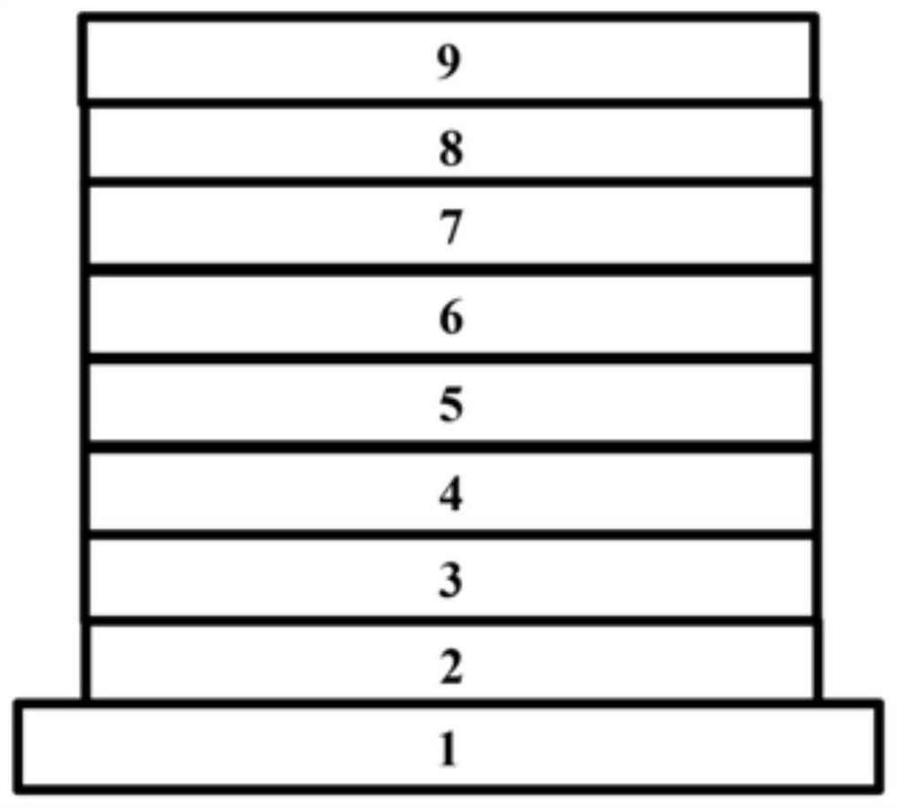
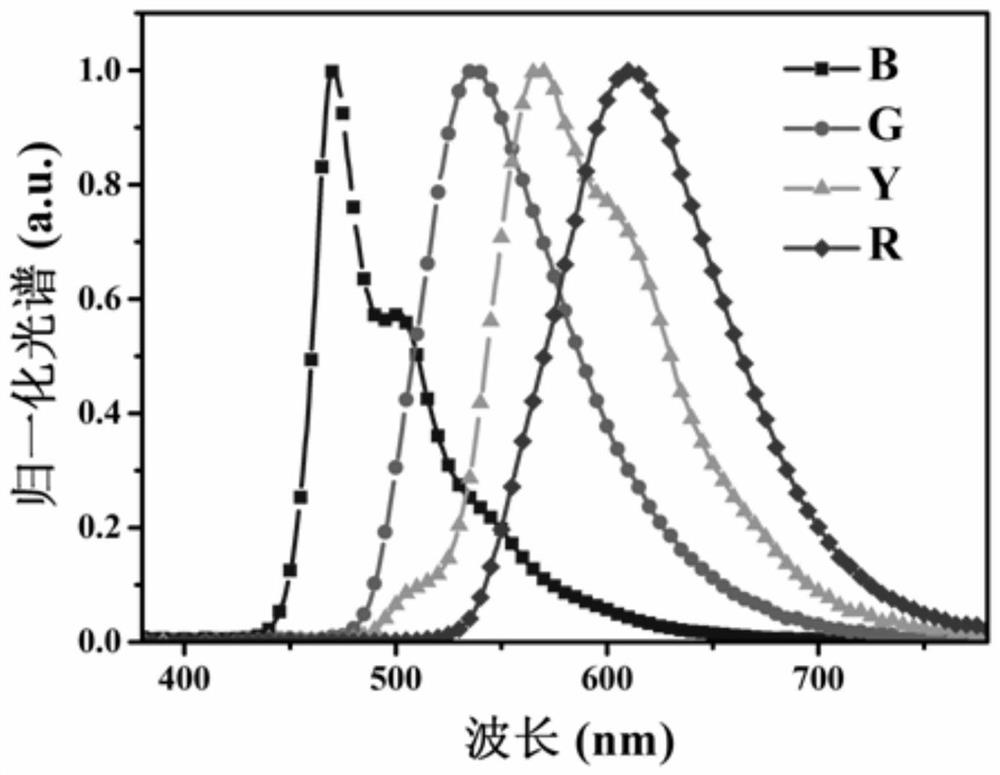
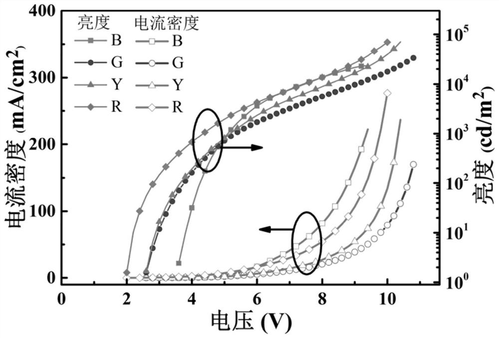
[0030] A kind of phosphorescence-sensitized fluorescent blue OLEDs (device B) of the present embodiment, at first clean 90 minutes ultrasonically to ITO conductive glass with cleaning agent, then rinse ITO conductive glass with deionized water, blow dry with nitrogen, put into oven to dry Baked for 30 minutes, then treated with ultraviolet ozone for 6 minutes, then put the ITO conductive glass into the vacuum coating machine, when the pressure of the vacuum coating system is lower than 1×10 -4 At Pa, the film deposition begins. Using a specific mask, sequentially evaporate the hole injection layer material HAT-CN, the hole transport layer material TAPC, the electron blocking layer material TCTA, and the light emitting layer material 26DCzPPy: 8wt% fac-Ir (iprpmi) on the ITO conductive glass 3: 1wt%TBPe, electron transport layer material TPBi, electron injection layer material LiF and cathode material Al. The rate and thickness of each functional layer evaporated are controlle...
Embodiment 2
[0032] A kind of phosphorescence-sensitized fluorescent OLEDs (device G) of the present embodiment, at first clean 90 minutes ultrasonically to ITO conductive glass with cleaning agent, then rinse ITO conductive glass with deionized water, blow dry with nitrogen, put into oven to bake 30 minutes, and then treated with ultraviolet ozone for 6 minutes and then put the ITO conductive glass into the vacuum coating machine. When the pressure of the vacuum coating system is lower than 1×10 -4 At Pa, the film deposition begins. Using a specific mask, on the ITO conductive glass, the hole injection layer material HAT-CN, the hole transport layer material TAPC, the electron blocking layer material TCTA and CDBP, and the light emitting layer material CDBP:PO-T2T:5wt%Ir were evaporated sequentially. (mppy) 3 : 1wt% TTPA, electron transport layer material PO-T2T, electron injection layer material LiF and cathode material Al. The rate and thickness of each functional layer evaporated ar...
Embodiment 3
[0034] A kind of phosphorescence-sensitized fluorescent OLEDs (device Y) of the present embodiment, at first clean 90 minutes ultrasonically to ITO conductive glass with cleaning agent, then rinse ITO conductive glass with deionized water, blow dry with nitrogen, put into oven to bake 30 minutes, and then treated with ultraviolet ozone for 6 minutes and then put the ITO conductive glass into the vacuum coating machine. When the pressure of the vacuum coating system is lower than 1×10 -4 At Pa, the film deposition begins. Using a specific mask, on the ITO conductive glass, the hole injection layer material HAT-CN, the hole transport layer material TAPC, the electron blocking layer material TCTA and mCBP, and the light emitting layer material mCBP:PO-T2T:9wt%Ir were sequentially evaporated. (ppy) 3 : 3wt% TBRb, electron transport layer material PO-T2T, electron injection layer material liF and cathode material Al. The rate and thickness of each functional layer evaporated are...
PUM
| Property | Measurement | Unit |
|---|---|---|
| thickness | aaaaa | aaaaa |
| thickness | aaaaa | aaaaa |
| thickness | aaaaa | aaaaa |
Abstract
Description
Claims
Application Information
 - R&D
- Intellectual Property
- Life Sciences
- Materials
- Tech Scout
- Unparalleled Data Quality
- Higher Quality Content
- 60% Fewer Hallucinations
Browse by: Latest US Patents, China's latest patents, Technical Efficacy Thesaurus, Application Domain, Technology Topic, Popular Technical Reports.
© 2025 PatSnap. All rights reserved.Legal|Privacy policy|Modern Slavery Act Transparency Statement|Sitemap|About US| Contact US: help@patsnap.com