Method for forming silicon film and method for manufacturing power storage device

Inactive Publication Date: 2013-01-10
SEMICON ENERGY LAB CO LTD
View PDF3 Cites 4 Cited by
  • Summary
  • Abstract
  • Description
  • Claims
  • Application Information

AI Technical Summary

Benefits of technology

The patent text describes a way to make a silicon film that is less likely to become powder and can be used as an active material layer in a power storage device. This method improves the cycle characteristics and increases the charge and discharge capacity of the device.

Problems solved by technology

However, when silicon is used as an active material layer of a power storage device, the silicon expands and contracts repeatedly due to repeated charge and discharge cycles.
As a result, the silicon turns into fine powder and separation or the like is caused, which deteriorates properties of the power storage device.
Therefore, even when silicon is used as an active material layer, it is difficult to obtain charge / discharge capacity as high as the theoretical capacity.

Method used


Image

  • Method for forming silicon film and method for manufacturing power storage device
  • Method for forming silicon film and method for manufacturing power storage device
  • Method for forming silicon film and method for manufacturing power storage device

Examples


embodiment 1

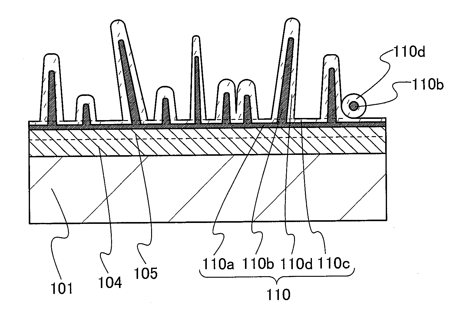
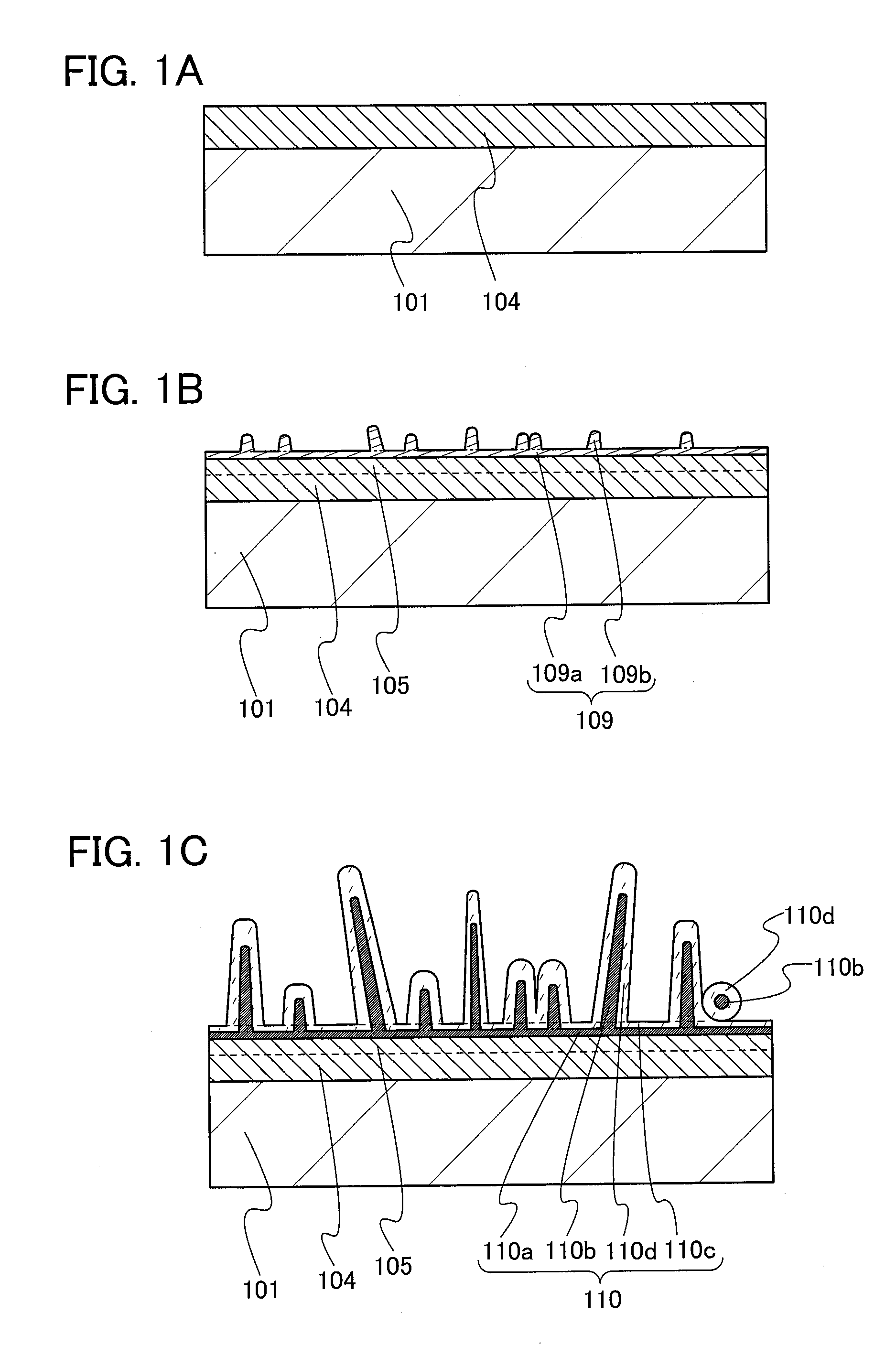
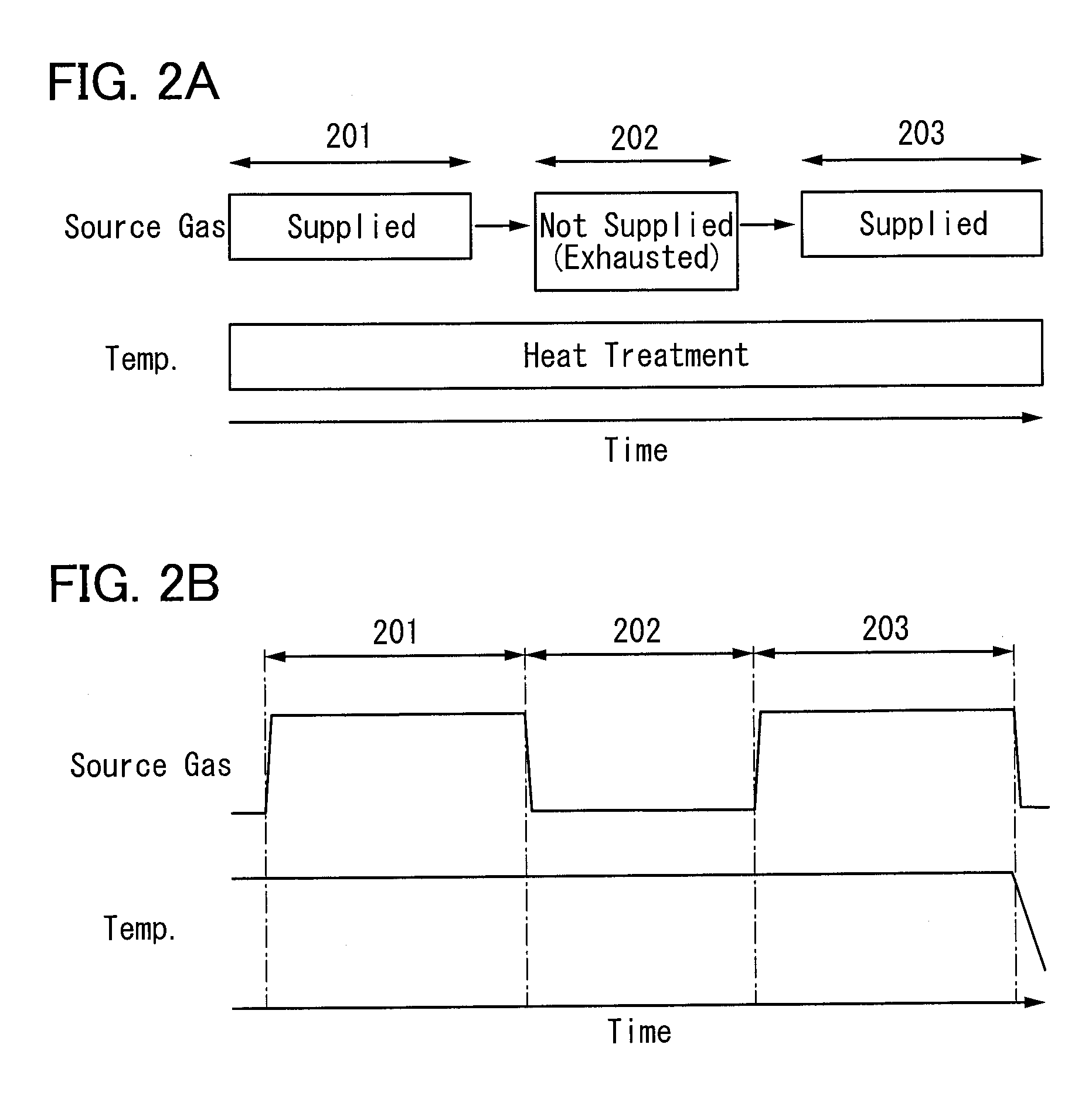
[0023]In this embodiment, a method for forming a silicon film according to one embodiment of the present invention and an example of applying the silicon film to an active material layer of a power storage device will be described with reference to drawings.

[0024]A conductive layer 104 is formed over a substrate 101 (see FIG. 1A). The conductive layer 104 can be formed using a conductive material and a method such as a printing method, a sol-gel method, a coating method, an ink-jet method, a CVD method, a sputtering method, or an evaporation method as appropriate. In addition, the conductive layer 104 may have a foil shape, a plate shape, a net shape, or the like. Note that in the case where the conductive layer 104 has a foil shape or a plate shape, it is not necessary to provide the substrate 101. In the case where the conductive layer 104 has a foil shape, roll-to-roll processing can be employed.

[0025]The conductive layer 104 is preferably formed using a metal element which forms...

embodiment 2

[0078]In this embodiment, a power storage device according to one embodiment of the present invention will be described.

[0079]The power storage device according to one embodiment of the present invention includes at least a positive electrode, a negative electrode, a separator, and an electrolyte. The negative electrode includes the silicon film according to Embodiment 1 as an active material layer.

[0080]The electrolyte is a nonaqueous solution containing an electrolyte salt or a solution containing an electrolyte salt. Any electrolyte salt can be used as the electrolyte salt as long as it contains carrier ions such as alkali metal ions, alkaline earth metal ions, beryllium ions, or magnesium ions. Examples of the alkali metal ions include lithium ions, sodium ions, and potassium ions. Examples of the alkaline earth metal ions include calcium ions, strontium ions, and barium ions. In this embodiment, an electrolyte salt containing lithium ions (hereinafter referred to as a lithium-c...

embodiment 3

[0111]The power storage device according to one embodiment of the present invention can be used for power supplies of a variety of electric appliances which can be operated with power.

[0112]Specific examples of electric appliances each utilizing the power storage device according to one embodiment of the present invention are as follows: display devices, lighting devices, desktop personal computers and laptop personal computers, image reproduction devices which reproduce still images and moving images stored in recording media such as digital versatile discs (DVDs), mobile phones, portable game machines, portable information terminals, e-book readers, video cameras, digital still cameras, high-frequency heating appliances such as microwave ovens, electric rice cookers, electric washing machines, air-conditioning systems such as air conditioners, electric refrigerators, electric freezers, electric refrigerator-freezers, freezers for preserving DNA, and medical electrical equipment su...


PUM

PropertyMeasurementUnit
Temperatureaaaaaaaaaa
Electrical conductoraaaaaaaaaa

Abstract

A formation method of a silicon film which contributes to improvements in cycle characteristics and an increase in charge / discharge capacity and can be used as an active material layer is provided. In addition, a manufacturing method of a power storage device including the silicon film is provided. The formation method is as follows. A crystalline silicon film is formed over a conductive layer by an LPCVD method. The supply of a source gas is stopped and heat treatment is performed on the silicon film while the source gas is exhausted. The silicon film is grown to have whisker-like portions by an LPCVD method while the source gas is supplied into the reaction space. A power storage device is manufactured using, as an active material layer included in a negative electrode, the silicon film grown to have whisker-like portions.

Description

BACKGROUND OF THE INVENTION[0001]1. Field of the Invention[0002]The present invention relates to a method for forming a silicon film and a method for manufacturing a power storage device including the silicon film.[0003]Note that the power storage device indicates every element and every device which have a function of storing power.[0004]2. Description of the Related Art[0005]In recent years, power storage devices such as lithium-ion secondary batteries, lithium-ion capacitors, and air cells have been developed.[0006]An electrode for such a power storage device is manufactured by forming an active material over a surface of a current collector. As the active material, a material which can store and release ions serving as carriers, such as carbon or silicon, is used. In addition, phosphorus-doped silicon has larger theoretical capacity than carbon and thus is advantageous in terms of increasing capacity of a power storage device (see Patent Document 1).[Reference][Patent Document 1...

Claims


Application Information

Patent Timeline
IPC IPC(8): C23C16/24
CPCC23C16/24C23C16/0281C23C16/56H01M4/134Y02E60/13H01M10/0525Y02E60/122H01G11/30H01G11/50H01M4/386Y02E60/10C23C16/06H01M4/1395H01M4/38H01M10/052
Inventor TAKEUCHI, TOSHIHIKOKURIKI, KAZUTAKAISHIKAWA, MAKOTO
Owner SEMICON ENERGY LAB CO LTD
Why Eureka
Try Eureka