
Method for manufacturing oxide semiconductor film, method for manufacturing semiconductor device, and semiconductor device

a manufacturing method and semiconductor technology, applied in the direction of semiconductor devices, basic electric elements, electrical apparatus, etc., can solve the problems of incomplete depletion of channel regions, amorphous regions remain, and regions near the interface with the base cannot be crystallized, so as to improve the properties and reliability of elements, improve the mobility of carriers

Active Publication Date: 2013-01-10
SEMICON ENERGY LAB CO LTD
View PDF9 Cites 30 Cited by
  • Summary
  • Abstract
  • Description
  • Claims
  • Application Information

AI Technical Summary

Benefits of technology

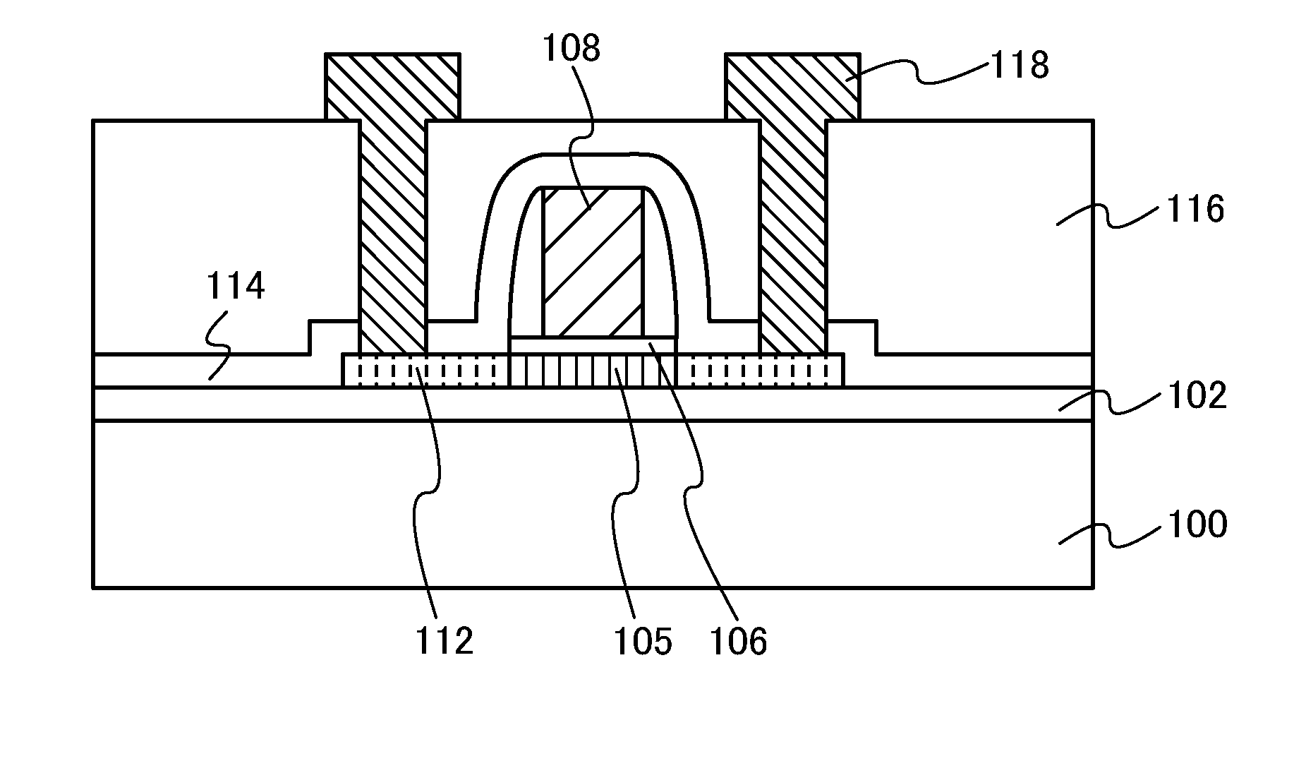
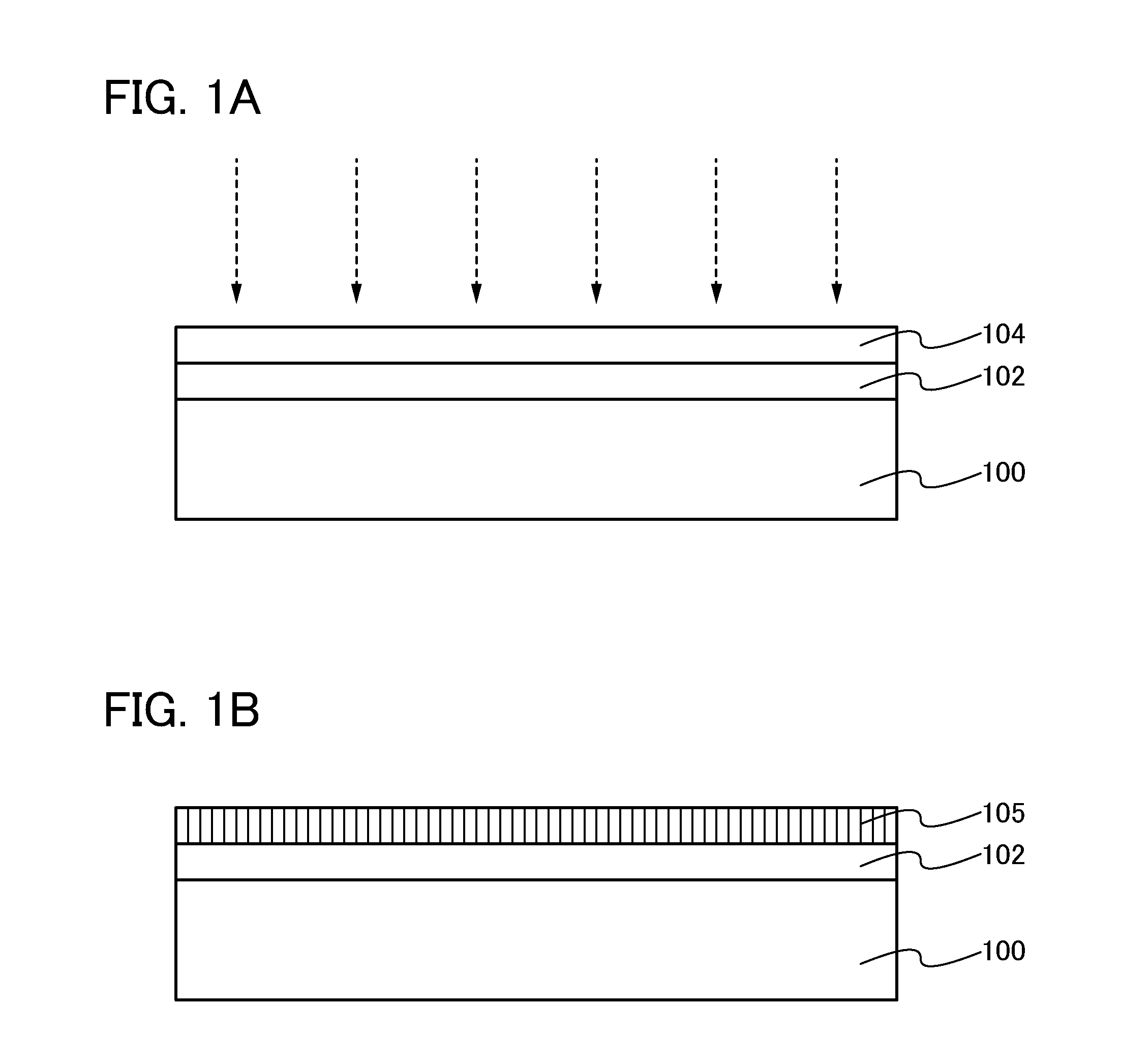
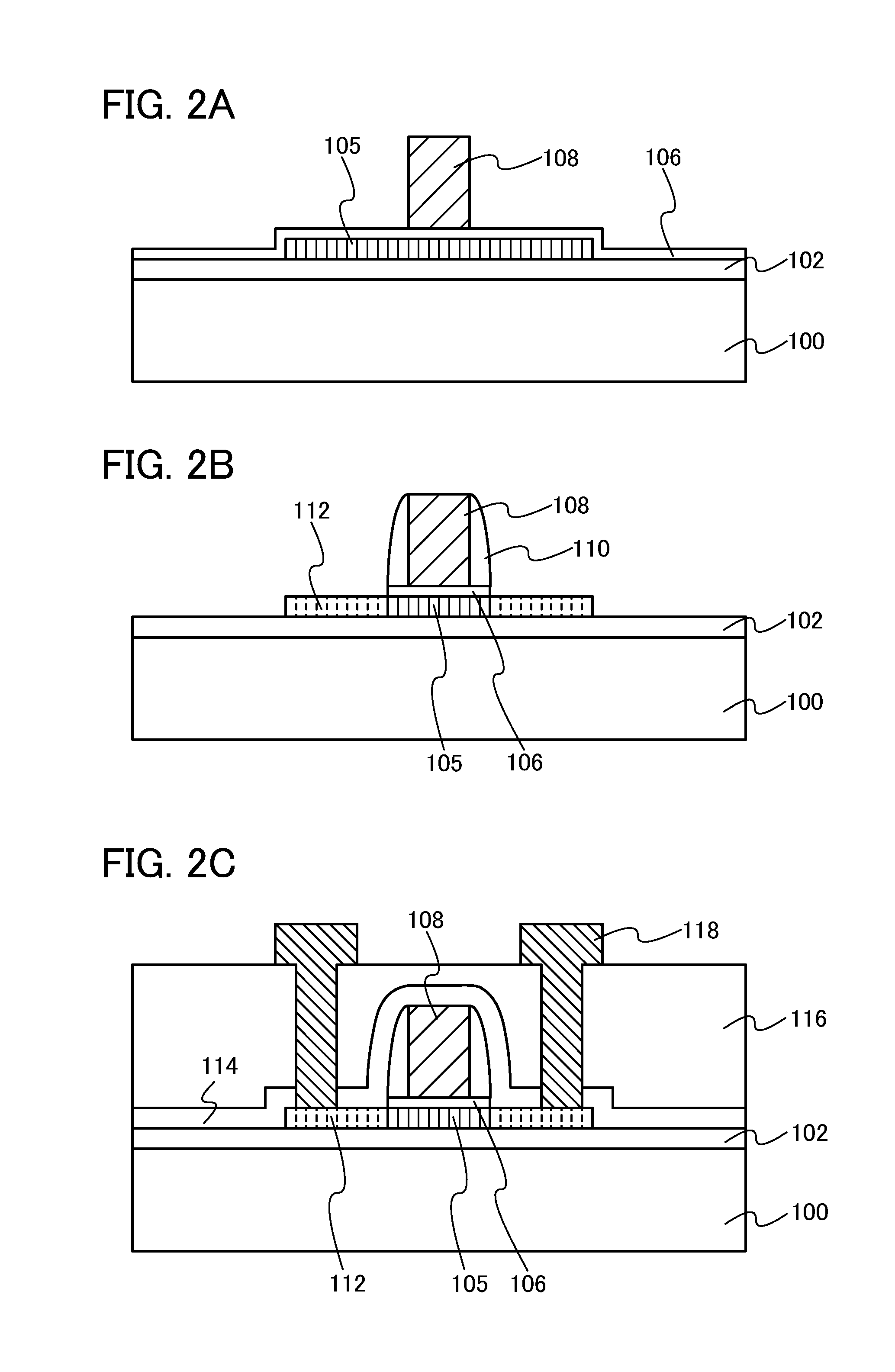
The patent text describes a method for improving the performance and reliability of transistors made from oxide semiconductor films. By using an energy beam, such as a laser beam, to crystallize the oxide semiconductor film, researchers have been able to create a more stable and efficient interface between the film and the base surface, as well as between an insulating film and the base surface. This has resulted in better carrier-transport properties and reduced power consumption. Additionally, the use of a higher melting point material for the base surface or film in contact with the oxide semiconductor film prevents contamination of the film during the crystallization process. Overall, this method provides a more reliable and efficient way to produce high-quality transistors using oxide semiconductor films.

Problems solved by technology

In crystallization of oxide semiconductors and other semiconductors, there is a problem in that an amorphous region remains in the vicinity of the interface between a base and a semiconductor layer to be crystallized.
In crystallization of an oxide semiconductor film formed on such an insulating material different from the oxide semiconductor, the problem arises in that a region near the interface with the base cannot be crystallized and an amorphous region remains.
In order to reduce parasitic capacitance and operate the transistor at low power consumption, however, the oxide semiconductor film needs to be made thin so that the channel region is completely depleted.
In that case, conventional techniques, which have difficulty in crystallizing the immediate vicinity of the interface with the base, prevent miniaturization of transistors.
Thus, even when the upper layer side of the oxide semiconductor film is crystallized, an amorphous region remains at the interface with the base insulating film, which has adversely affected the characteristics of transistors and the like.

Method used


Image

  • Method for manufacturing oxide semiconductor film, method for manufacturing semiconductor device, and semiconductor device
  • Method for manufacturing oxide semiconductor film, method for manufacturing semiconductor device, and semiconductor device
  • Method for manufacturing oxide semiconductor film, method for manufacturing semiconductor device, and semiconductor device

Examples


example 1

[0097]In this example, an oxide semiconductor film according to one embodiment of the present invention is formed and observed using a transmission electron microscope (TEM), and the results thereof will be described.

[0098]In this example, a sample A was manufactured: a silicon oxide film (with a thickness of 300 nm) was deposited over a glass substrate (AN100 manufactured by Asahi Glass Co., Ltd.), an aluminum oxide film (with a thickness of 20 nm) was deposited over the silicon oxide film, and an IGZO film (with a thickness of 30 nm) was deposited as an oxide semiconductor film over the aluminum oxide film. As a comparative example, a sample B was manufactured: a silicon oxide film (with a thickness of 300 nm) was deposited over a glass substrate (AN100 manufactured by Asahi Glass Co., Ltd.), and an IGZO film (with a thickness of 30 nm) was deposited as an oxide semiconductor film over the silicon oxide film.

[0099]That is to say, in the sample A, the aluminum oxide film serves as ...

example 2

[0114]In this example, an oxide semiconductor film according to one embodiment of the present invention is formed, the oxide semiconductor film is observed using a TEM and analyzed by electron diffraction measurement, and the results will thereof be described.

[0115]In this example, a sample C was manufactured: a silicon oxide film (with a thickness of 300 nm) was deposited over a glass substrate (AN100 manufactured by Asahi Glass Co., Ltd.), an yttria-stabilized zirconia (YSZ) film (with a thickness of 10 nm) was deposited over the silicon oxide film, and an IGZO film (with a thickness of 20 nm) was deposited as an oxide semiconductor film over the YSZ film.

[0116]That is to say, in the sample C, the YSZ film serves as a base insulating film of the IGZO film.

[0117]Manufacturing process of the sample C will be described below.

[0118]First, a silicon oxide film was formed over a glass substrate so as to have a thickness of 300 nm. The silicon oxide film was deposited by sputtering under...


PUM

PropertyMeasurementUnit
melting pointaaaaaaaaaa

Abstract

In an oxide semiconductor film formed over an insulating surface, an amorphous region remains in the vicinity of the interface with the base, which is thought to cause a variation in the characteristics of a transistor and the like. A base surface or film touching the oxide semiconductor film is formed of a material having a melting point higher than that of a material used for the oxide semiconductor film. Accordingly, a crystalline region is allowed to exist in the vicinity of the interface with the base surface or film touching the oxide semiconductor film. An insulating metal oxide is used for the base surface or film touching the oxide semiconductor film. The metal oxide used here is an aluminum oxide, gallium oxide, or the like that is a material belonging to the same group as the material of the oxide semiconductor film.

Description

BACKGROUND OF THE INVENTION[0001]1. Field of the Invention[0002]The present invention relates to an oxide semiconductor and a semiconductor device including a transistor using the oxide semiconductor in a channel region.[0003]2. Description of the Related Art[0004]An oxide semiconductor has attracted attention as a material for transistors. The oxide semiconductor is said to have a feature similar to that of amorphous silicon capable of being formed at a low temperature, and a feature similar to that of polycrystalline silicon having high field-effect mobility. For example, the following is disclosed: a field-effect transistor using an amorphous oxide, whose electron carrier concentration is controlled, and an image display device using the transistor (Patent Document 1).[0005]The transistor using an amorphous oxide semiconductor formed at room temperature, however, has a problem in characteristics: not enough high field-effect mobility, low reliability, and large hysteresis. In ord...

Claims


Application Information

Patent Timeline
Patent Type & Authority Applications(United States)
IPC IPC(8): H01L21/36H01L29/12
CPCH01L21/02422H01L21/02488H01L21/02554H01L21/02565H01L29/66969H01L21/02686H01L29/78603H01L29/78606H01L29/7869H01L21/02631
Inventor KOYAMA, MASAKINEI, KOSEISHIMOMURA, AKIHISAHONDO, SUGURUHASEGAWA, TORU
Owner SEMICON ENERGY LAB CO LTD
Learn More