
Plasma display panel

a technology of display panels and plasma, applied in the direction of electric discharge tubes, gas-filled discharge tubes, electrical apparatus, etc., can solve the problems of reduced discharge time, reduced image quality, lighting failure, etc., to improve secondary electron emission characteristics, reduce discharge starting voltage, and increase brightness

Inactive Publication Date: 2012-12-20
MIURA MASANORI +2
View PDF0 Cites 0 Cited by
  • Summary
  • Abstract
  • Description
  • Claims
  • Application Information

AI Technical Summary

Benefits of technology

[0022]According to this feature, the protective layer can have improved secondary electron emission characteristics, which makes it possible to reduce discharge starting voltage even when the partial pressure of xenon (Xe) in discharge gas is increased to increase brightness, and also makes it possible to provide a high display performance PDP that is reduced in discharge delay and prevented from causing lighting failure even when displaying high-definition images and to provide a PDP that can be driven with high brightness at low voltage even when displaying high-definition images.

Problems solved by technology

Unfortunately, a time lag called “discharge delay” occurs between the voltage pulse rise and the generation of discharge in the discharge space, and therefore, as the pulse width decreases, the possibility of completing discharge within the writing period decreases.
This can cause lighting failure and the problem of a reduction in image quality, such as flicker.
In this case, discharge voltage increases, and discharge delay also increases, so that the problem of a reduction in image quality, such as lighting failure also occurs.
Therefore, in making high-definition, low-power-consumption PDPs, there has been a challenge to achieve both prevention of an increase in discharge voltage and lighting failure reduction to improve image quality.
Unfortunately, when a protective layer is doped with an impurity so that electron emission characteristics can be improved, charges decrease with time at a higher attenuation rate in the process of storing charges on the surface of a protective layer for use as a memory function part.
On the other hand, in the case where magnesium oxide (MgO) crystal particles are formed on a magnesium oxide (MgO) protective layer, discharge delay can be reduced so that lighting failure can be reduced, but there is a problem in which discharge voltage cannot be reduced.

Method used


Image

  • Plasma display panel
  • Plasma display panel
  • Plasma display panel

Examples


first exemplary embodiment

[0033]Hereinafter, a description is given of a PDP according to a first exemplary embodiment of the present invention.

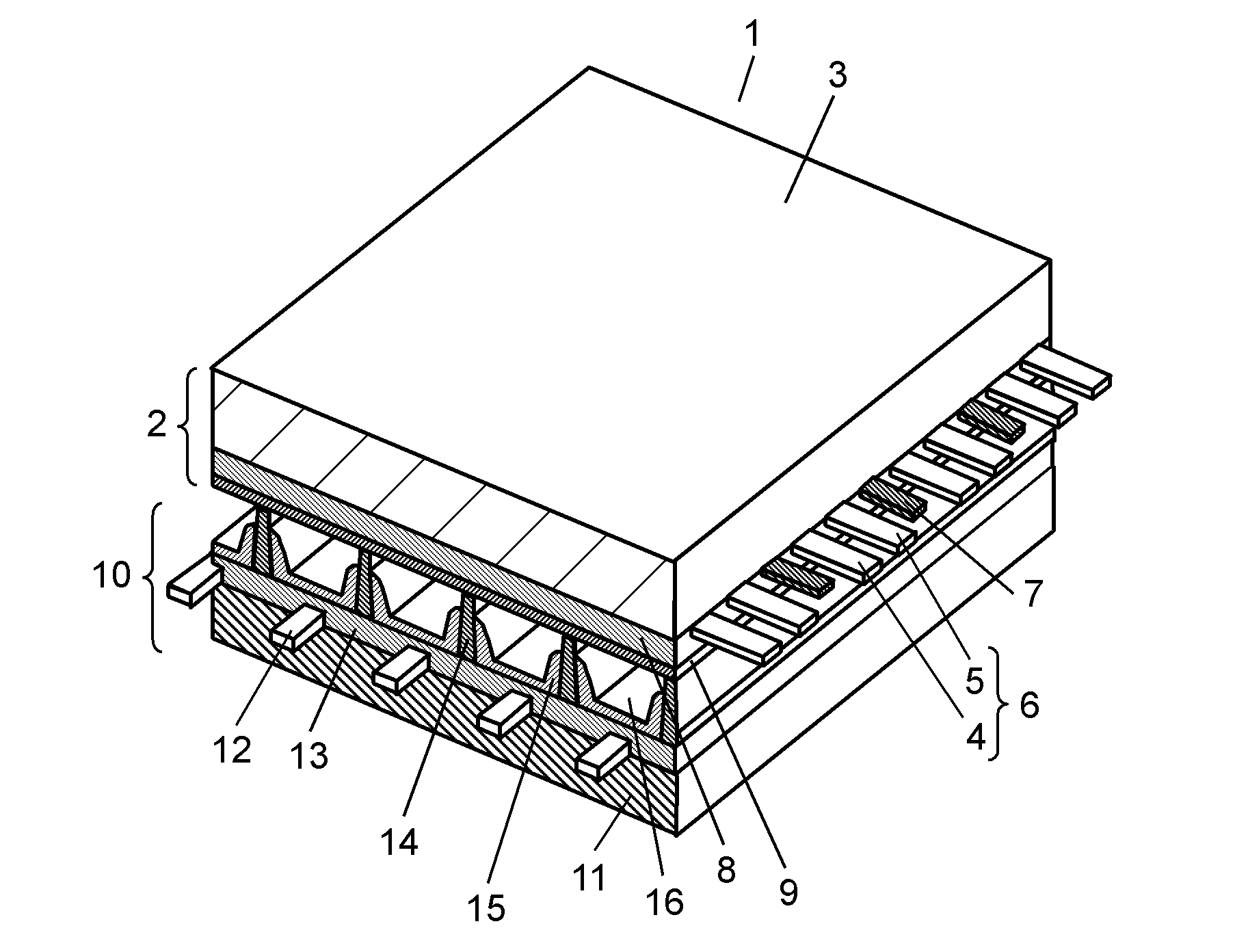
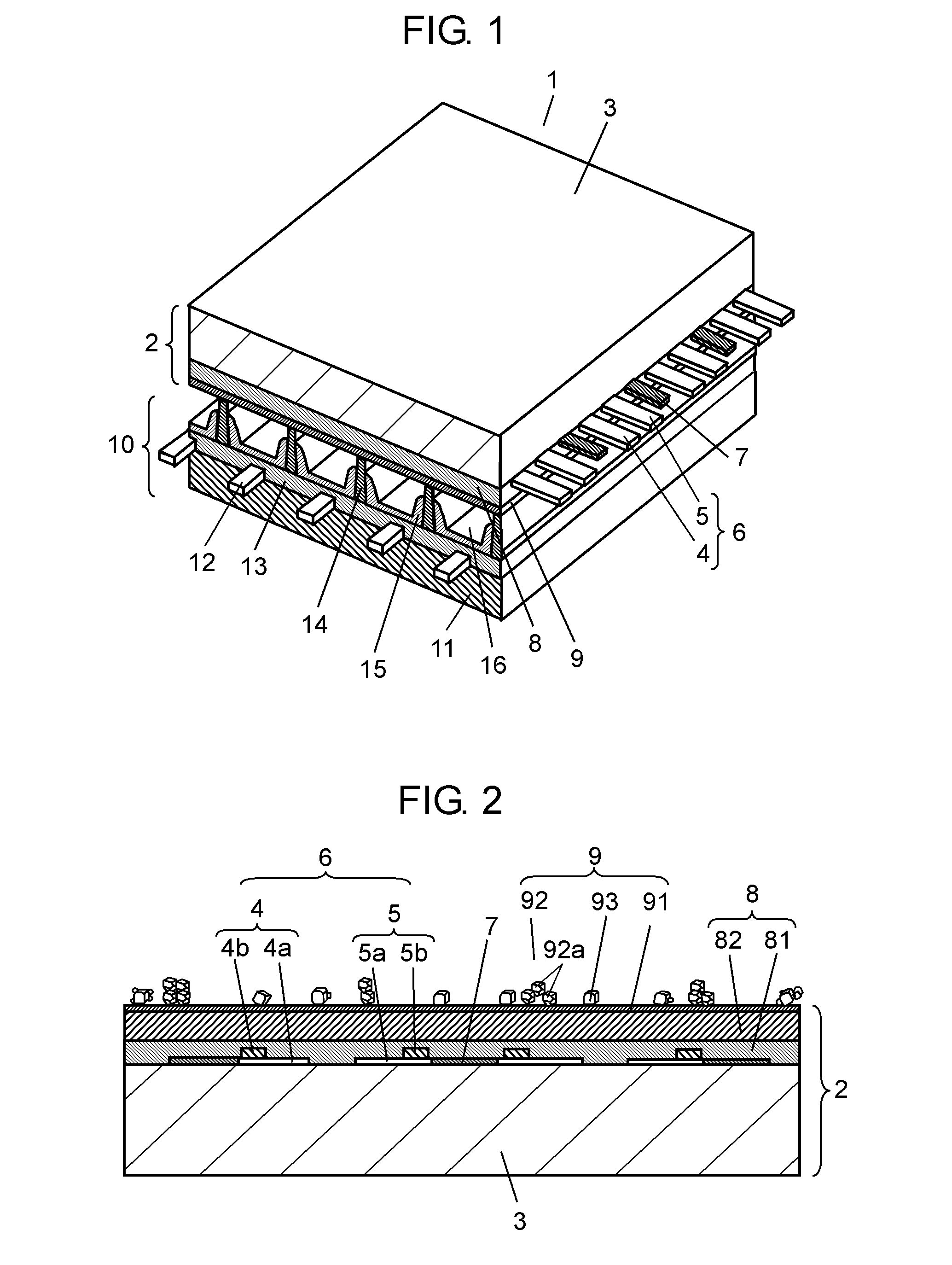
[0034]FIG. 1 is a perspective view showing the structure of a PDP according to an embodiment of the present invention. PDP 1 has the same basic structure as that of a general AC surface-discharge PDP. As shown in FIG. 1, PDP 1 includes: front plate 2 including front glass substrate 3 and other components; rear plate 10 including rear glass substrate 11 and other components, which is opposed to front plate 2; and a sealing material made of a glass frit or the like, with which the periphery thereof is hermetically sealed. Discharge gas such as xenon (Xe) and neon (Ne) is sealed at a pressure between 400 Torr and 600 Torr (5.3×10⁴ Pa and 8.0×10⁴ Pa) in discharge space 16 inside sealed PDP 1.

[0035]In front plate 2, strip-shaped display electrodes 6 each including a set of scan electrode 4 and sustain electrode 5 and black stripes (light-shielding layers) 7 are arranged i...

second exemplary embodiment

[0115]Hereinafter, a description is given of a PDP according to a second exemplary embodiment of the present invention. The description of the same components as those in the first exemplary embodiment will be omitted.

[0116]While base layer 91 made of magnesium oxide (MgO) is used in the PDP according to the first exemplary embodiment, base layer 91 containing at least two metal oxides selected from the group consisting of magnesium oxide, calcium oxide, strontium oxide, and barium oxide is used in the PDP according to the second exemplary embodiment.

[0117]Next, a detailed description is given of protective layer 9 in this embodiment.

[0118]Protective layer 9 includes: base layer 91 formed on dielectric layer 8; aggregate particles 92 each including an aggregate of a plurality of magnesium oxide (MgO) crystal particles 92a deposited on base layer 91; and metal oxide particles 93 deposited on base layer 91. Base layer 91 and metal oxide particles 93 are made of metal oxides including ...


PUM

PropertyMeasurementUnit
pressureaaaaaaaaaa
pressureaaaaaaaaaa
pressureaaaaaaaaaa

Abstract

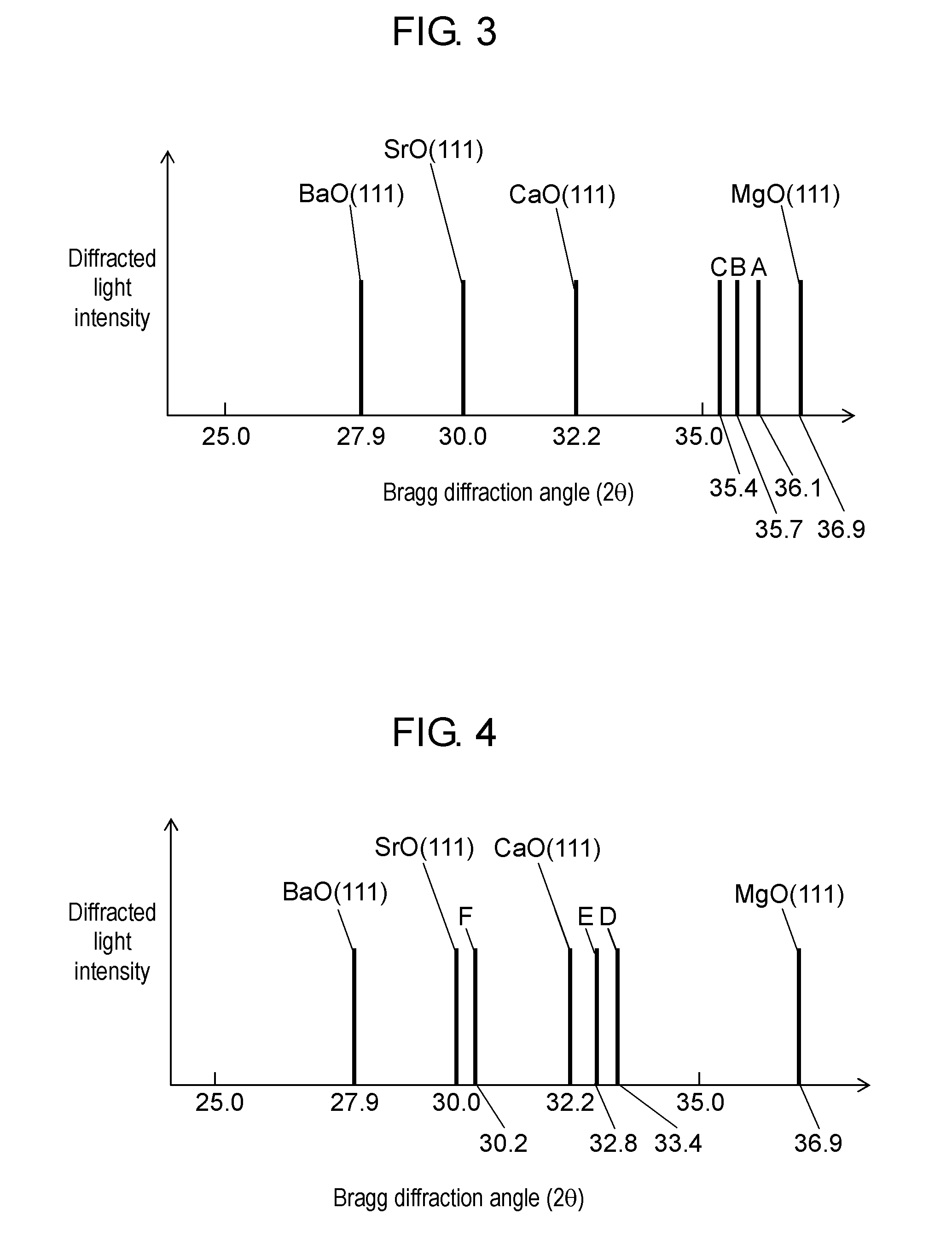
A plasma display has a protective layer (9) including a base layer (91) over which aggregate particles (92) each including an aggregate of a plurality of magnesium oxide crystal particles (92a) and metal oxide particles (93) are scattered. The metal oxide particles (93) contain at least two metal oxides selected from the group consisting of magnesium oxide, calcium oxide, strontium oxide, and barium oxide. X-ray diffraction analysis of the metal oxide particles (93) shows a diffraction peak of a specific crystal plane between a diffraction peak of the specific crystal plane of one of the two metal oxides and a diffraction peak of the specific crystal plane of another one of the two metal oxides.

Description

TECHNICAL FIELD[0001]The present invention relates to plasma display panels for use in display devices, etc.[0002]BACKGROUND ART[0003]Plasma display panels (hereinafter referred to as “PDPs”), which can have a high-definition and large screen, have been commercialized as 100-inch class televisions, etc. In recent years, PDPs have found application in high-definition television systems in which the number of scanning lines is twice or more than that of the conventional NTSC system, and there also has been an increasing demand for a lead-free PDP in view of environmental problems and measures to further reduce power consumption in response to energy problems.[0004]The PDP basically includes a front plate and a rear plate. The front plate includes a glass substrate that is formed of sodium borosilicate-based glass by float glass process, display electrodes each composed of stripe-shaped transparent and bus electrodes, which are formed on one main surface of the glass substrate, a diele...

Claims


Application Information

Patent Timeline
Patent Type & Authority Applications(United States)
IPC IPC(8): H01J17/49H01J11/12H01J11/40
CPCH01J11/40H01J11/12
Inventor MIURA, MASANORITSUJITA, TAKUJIGOTOU, MASASHI
Owner MIURA MASANORI
Learn More