
Lighting Device and Method for Manufacturing the Same

Inactive Publication Date: 2012-12-13
SEMICON ENERGY LAB CO LTD
View PDF3 Cites 17 Cited by
  • Summary
  • Abstract
  • Description
  • Claims
  • Application Information

AI Technical Summary

Benefits of technology

[0011]Patent. Document 2 discloses a peripheral sealing layer which includes an ultraviolet curable resin and which is used to fix an element substrate provided with an organic EL element and a sealing substrate to each other. An adhesive layer including a thermosetting resin is provided in a portion enclosed by the peripheral sealing layer. An organic buffer layer covering an organic EL layer and a gas barrier layer covering the organic buffer layer are provided under the peripheral sealing layer. Such a sealing structure is proposed in which the organic buffer layer prevents damage to the gas barrier layer and the gas barrier layer prevents entry of moisture or the like from the outside air.
[0014]In view of the above problems, a lighting device is formed using a light-emitting element (organic EL element) by a more simplified method in one embodiment of the present invention. Further, an object of one embodiment of the present invention is to provide a highly reliable lighting device and a method for manufacturing the lighting device by increasing the adhesion of a sealing region of the light-emitting element.
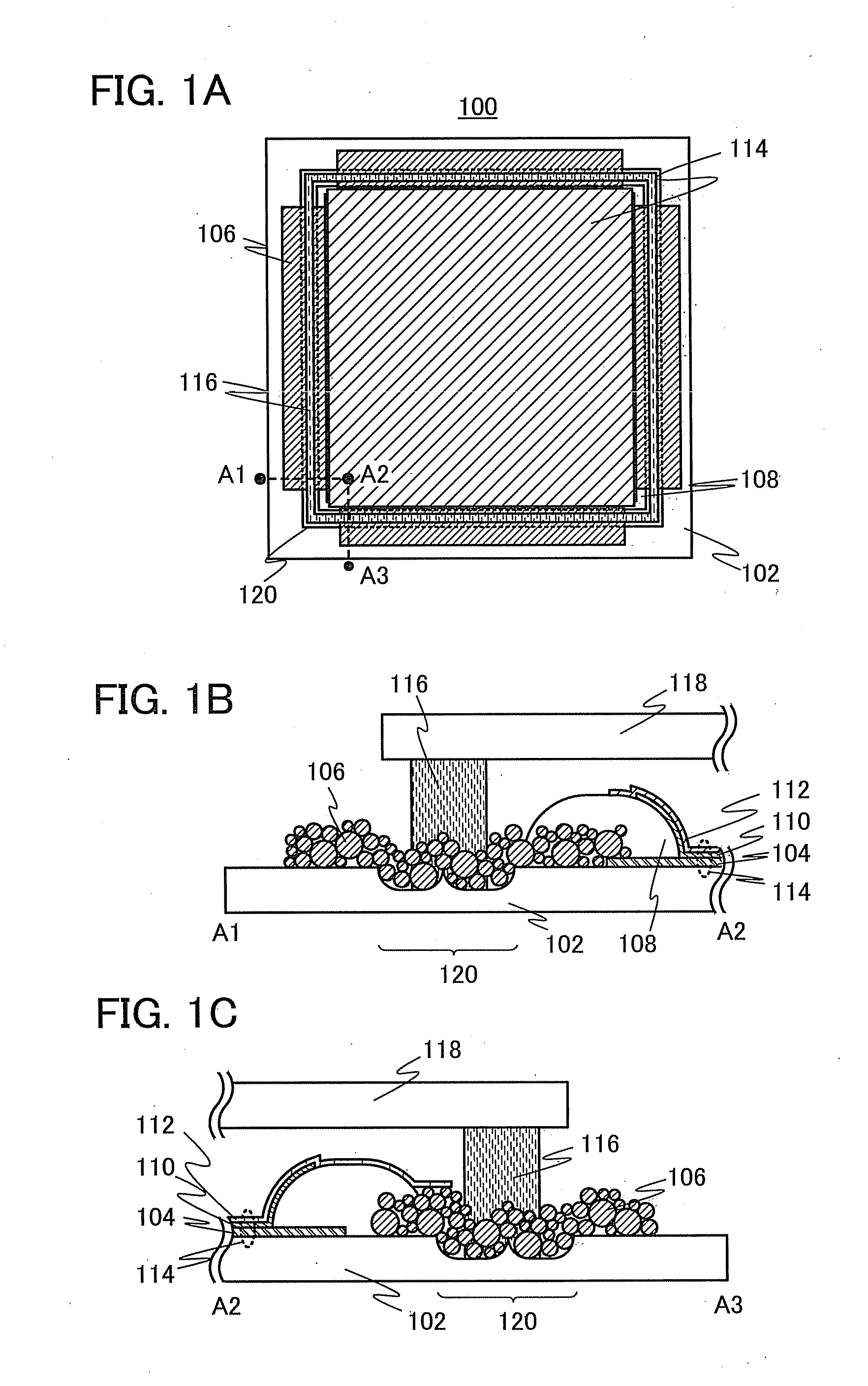
[0017]In the above structure, the sealant is in contact with the uneven region formed around the periphery of the light-emitting element and the conductive paste formed over the uneven region; thus, the adhesion area can be increased and the adhesion can be increased. Note that the conductive paste has a rough surface owing to conductive particles included therein, which is very suitable for increasing the adhesion area.
[0019]In the above structure, the sealant is in contact with the uneven region around the periphery of the light-emitting element and the conductive paste formed over the uneven region; thus, the adhesion area can be increased and the adhesion can be increased. Note that the conductive paste has a rough surface owing to conductive particles included therein, which is very suitable for increasing the adhesion area. The light-emitting element is formed over the planarizing resin formed over the uneven region. The planarizing resin formed over the uneven region can diffuse light emitted from the light-emitting element, thereby improving the light extraction efficiency of the light-emitting element.
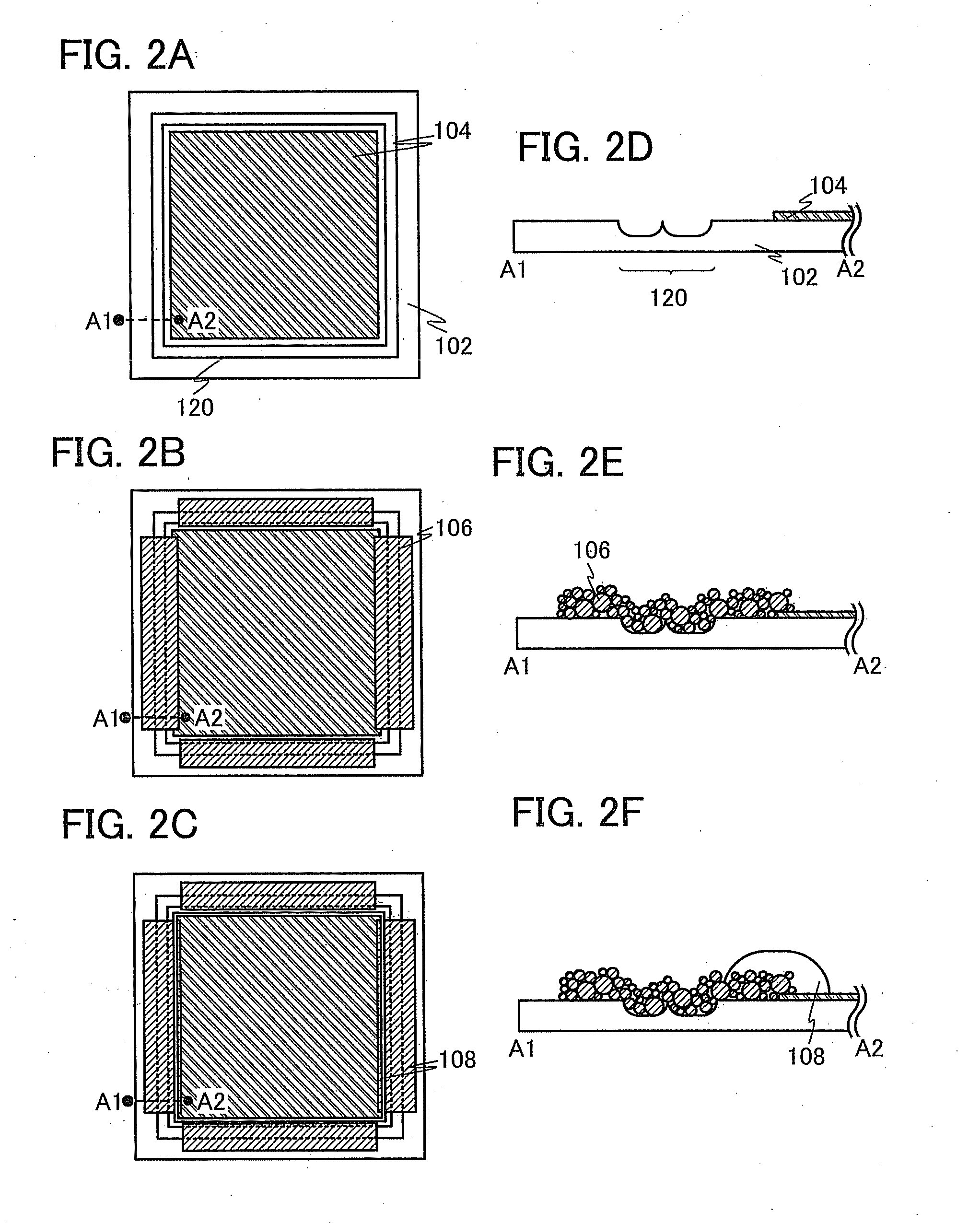
[0023]In the above manufacturing method, a pattern is preferably formed not through a patterning process by photolithography but by an evaporation method with the use of a metal mask, a screen printing method, or the like. By pattern formation without the use of photolithography as described above, the numbers of patterning steps and etching steps can be reduced; thus, a lighting device can be manufactured through a more simplified process. In addition, by reducing patterning steps and etching steps, manufacturing cost can be decreased.
[0024]According to the present invention, it is possible to provide a highly reliable lighting device and a method for manufacturing the lighting device by a more simplified method.

Problems solved by technology

However, the above method needs many steps such as a patterning step and an etching step to form the organic buffer layer and the gas barrier layer in desired regions, which leads to problems such as a considerably large number of steps and a high manufacturing cost.
Even when such structures are used, they are not sufficient to reduce the entry of moisture or oxygen from the outside.

Method used


Image

  • Lighting Device and Method for Manufacturing the Same
  • Lighting Device and Method for Manufacturing the Same
  • Lighting Device and Method for Manufacturing the Same

Examples


embodiment 1

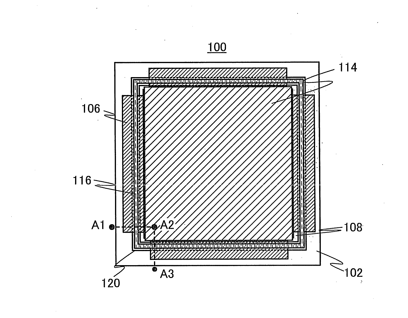
[0035]One embodiment of the present invention will be described with reference to FIGS. 1 A to 1C. FIG. 1A shows a top view of a lighting device 100. FIG. 1B is a cross-sectional view along the dashed line A1-A2 in FIG. 1A. FIG. 1C is a cross-sectional view along the dashed line A2-A3 in FIG. 1A. Note that in FIG. 1A, some of components (e.g., a sealing substrate 118) are not shown to avoid complexity of the drawing.

[0036]The lighting device 100 shown in FIGS. 1A to 1C includes a substrate 102, an uneven region 120 formed in the substrate 102, a first electrode 104 formed over the substrate 102, a connection electrode 106 formed over the substrate 102, the uneven region 120, and the first electrode 104, a partition wall 108 covering the first electrode 104 and the connection electrode 106, a light-emitting layer 110 formed over the first electrode 104 and the partition wall 108, a second electrode 112 formed over the partition wall 108, the light-emitting layer 110, and a connection...

embodiment 2

[0075]In this embodiment, an embodiment different from the lighting device 100 described in Embodiment 1 will be described with reference to FIGS. 4A to 4C. Note that the same reference numerals are used for the same parts as those in FIGS. 1A to 1C, and description thereof will not be repeated.

[0076]FIG. 4A shows a top view of a lighting device 200. FIG. 4B is a cross-sectional view along the dashed line B1-B2 in FIG. 4A. FIG. 4C is a cross-sectional view along the dashed line B2-B3 in FIG. 4A. Note that in FIG. 4A, some of components (e.g., the sealing substrate 118) are not shown to avoid complexity of the drawing.

[0077]The lighting device 200 shown in FIGS. 4A to 4C includes the substrate 102, a microlens array substrate 124, an uneven region 120a formed in the substrate 102, a planarizing resin 122 formed over the substrate 102, the first electrode 104 formed over the planarizing resin 122, the connection electrode 106 formed over the substrate 102, the planarizing resin 122, a...

embodiment 3

[0096]In this embodiment, an example of an element structure of a light-emitting element exhibiting organic EL emission which is used in the lighting device of one embodiment of the present invention will be described. The light-emitting element exhibiting the organic EL emission generates a smaller amount of heat than an LED. Thus, an organic resin can be used for a housing, so that a reduction in weight of the lighting device is possible, which is preferable.

[0097]A light-emitting element illustrated in FIG. 6A includes a first electrode 104, a light-emitting layer 110 over the first electrode 104, and a second electrode 112 over the light-emitting layer 110.

[0098]The light-emitting layer 110 includes at least a light-emitting layer containing a light-emitting organic compound. In addition, the light-emitting layer 110 can have a stacked-layer structure in which a layer containing a substance having a high electron-transport property, a layer containing a substance having a high h...


PUM


Abstract

A lighting device is formed using a light-emitting element by a more simplified method. The lighting device includes a light-emitting element including a light-emitting layer between a first electrode and a second electrode, a substrate provided with the light-emitting element and an uneven region around the periphery of the light-emitting element, a sealing substrate facing the substrate, connection electrodes connected to the first electrode and the second electrode and formed over the uneven region, and a sealant for bonding the substrate and the sealing substrate. The connection electrodes are each formed using a conductive paste, and the sealant is in contact with the connection electrodes and the uneven region provided around the periphery of the light-emitting element.

Description

BACKGROUND OF THE INVENTION[0001]1. Field of the Invention[0002]The present invention relates to a lighting device including an organic EL element and a method for manufacturing the lighting device.[0003]2. Description of the Related Art[0004]In recent years, a light-emitting element (also referred to as an organic electroluminescent (EL) element) in which a light-emitting layer containing an organic compound is provided between a pair of electrodes has been actively developed. Lighting has attracted attention as one of application fields of the light-emitting element. This is because an organic. EL element can be thin and light and enables surface emission, which provides features that differ from those of other lighting devices.[0005]Since an organic EL element can be formed in the form of a film, an element with a large area can be easily formed. A variety of researches has been conducted on lighting devices including organic EL elements (e.g., see Patent Document 1).[0006]Howeve...

Claims


Application Information

Patent Timeline
IPC IPC(8): H01L33/58
CPCH01L51/5203H01L51/5212H01L2251/5369H01L51/5275H01L51/5246H10K50/814H10K50/805H10K50/8426H10K50/858H10K2102/331F21V17/00H05B33/00
Inventor YOKOYAMA, KOHEIIKEDA, HISAOHIRASA, SHINICHI
Owner SEMICON ENERGY LAB CO LTD
Learn More