Semiconductor memory device
a memory device and semiconductor technology, applied in the direction of fault response, redundant data error correction, instruments, etc., can solve problems such as reading disturb, and achieve the effect of efficient data detection
- Summary
- Abstract
- Description
- Claims
- Application Information
AI Technical Summary
Benefits of technology
Problems solved by technology
Method used
Image

Examples
first embodiment
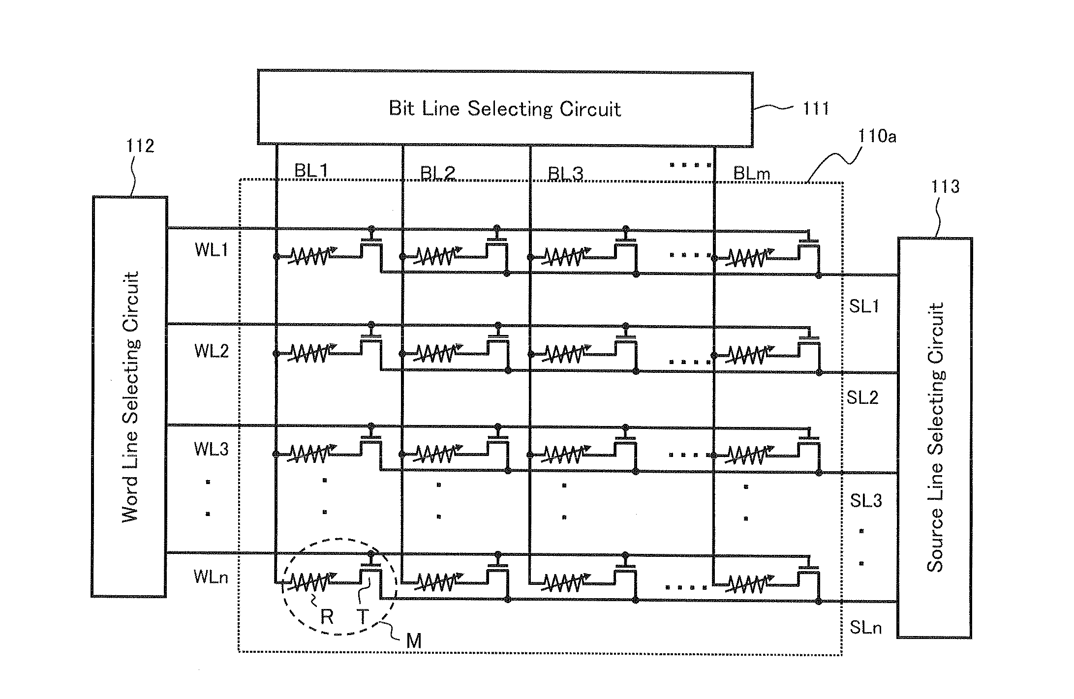
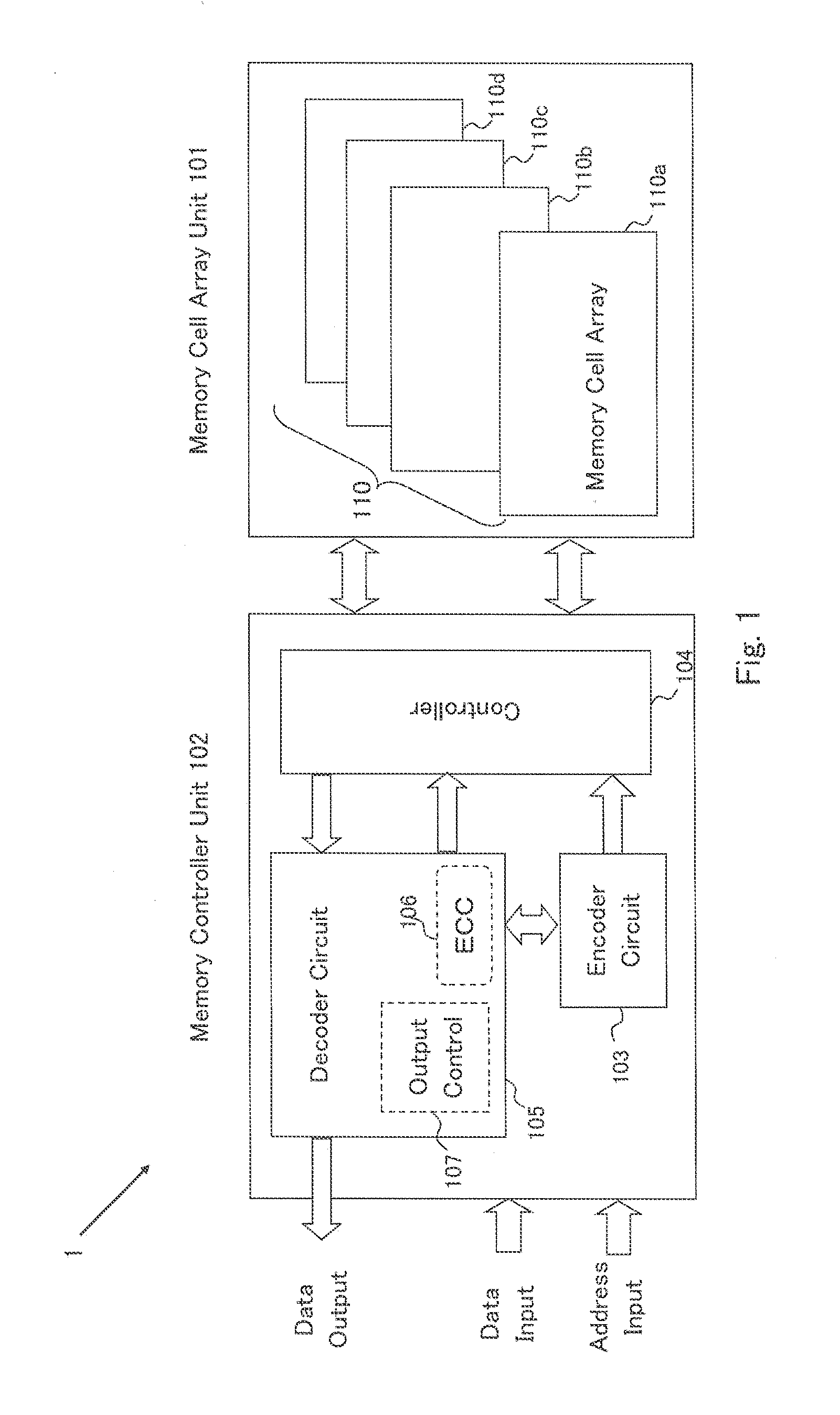
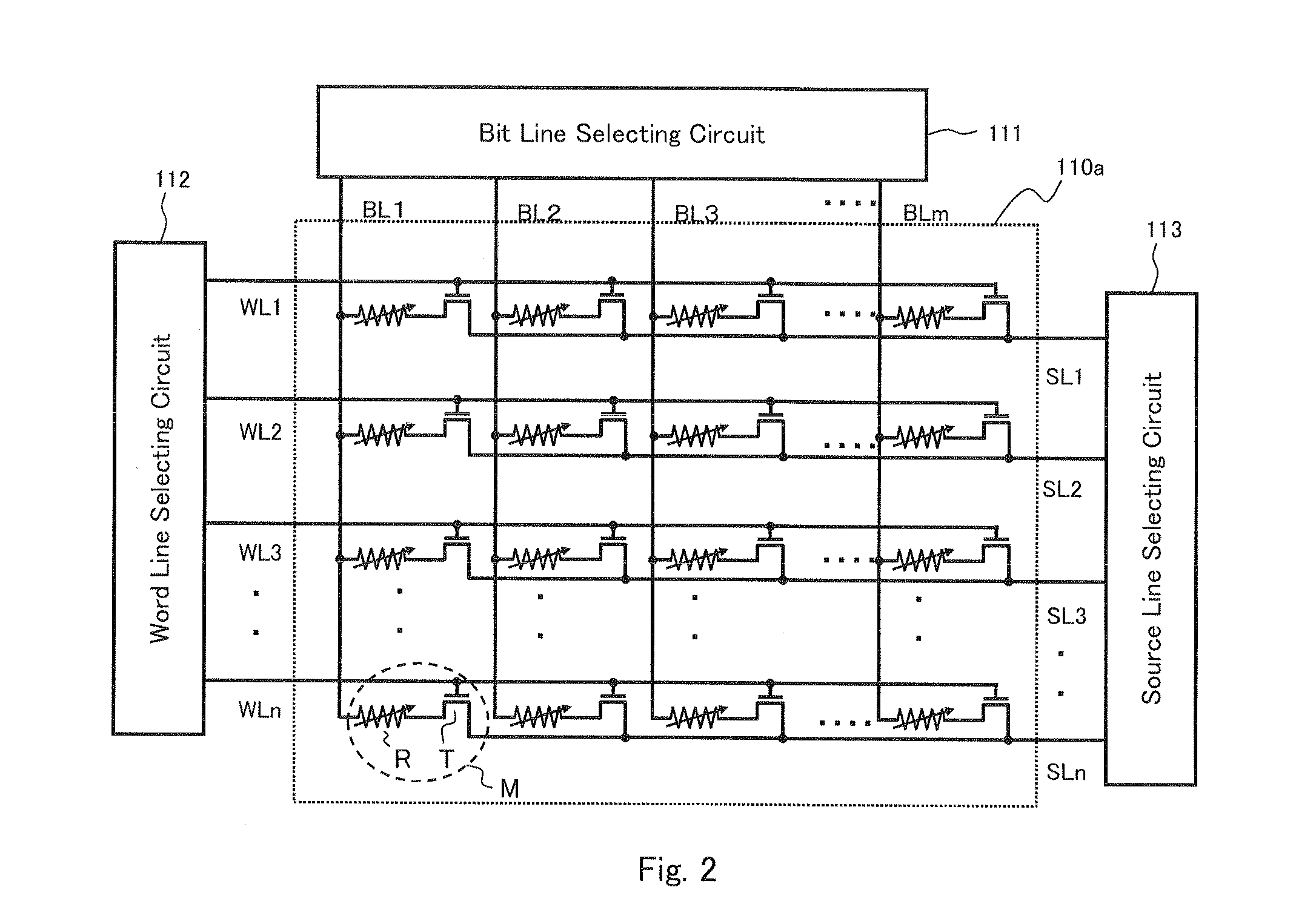
[0063]FIG. 1 shows a schematic circuit structure of a semiconductor memory device (hereinafter appropriately referred to as “present device 1”) according to one embodiment of the present invention. The present device 1 basically includes a memory cell array unit 101, and a memory controller unit 102. The memory controller unit 102 includes an encoder circuit 103 that performs error-correction coding for adding an error-correction check bit to a plurality of information bits, which are input data, and generates coded data having a bit length longer than that of the information bit; a controller 104 that controls a writing action and a reading action of the coded data to a memory cell in the memory cell array in the memory cell array unit 101 specified by an input address; and a decoder circuit 105 that decodes the coded data (information bit+check bit) read through the controller 104, detects whether the decoded data has an error or not, and corrects the error. The decoder circuit 10...
second embodiment
[0085]As described above, when the read data is decoded, and the error data is detected, the present device 1 executes the second writing action to the error data in the memory cell array based upon the error-correction code, thereby being capable of correcting the error with a high speed. However, it takes time to actually output true data after the detection of the error data. This is because the true data is outputted after the action in which the writing action is performed to correct the error data in the memory cell array, and then, the reading action is performed again, and the reading action, the decoding action, and the error correcting action are repeated until the error data is eliminated.
[0086]However, when the error data is detected, an error bit is specified out of the read data based upon the error-correction code, and the output control circuit 107 inverts the data of the error bit in the read data so as to output the true data. With this process, a high-speed data r...
third embodiment
[0091]FIG. 5 shows a timing chart of the reading action in the present device 1 provided with a plurality of banks. In FIG. 5, when the data stored in the memory cell array 110 is outputted, a sequence including five actions, which are an address input (A), a reading action (R), a decoding action (D), an error detecting action (E), and a correction and read / output action (W / O), is performed as one cycle each in the action cycle of a control clock. The respective action sequences correspond to the respective actions in steps #200 to #203, and #205 in FIG. 4.
[0092]In FIG. 5, in the respective action cycles t1 to t16, each action is ended with one clock of the control clock. However, there may be the case in which a plurality of clocks of the control clock are required for each action. In this case, the time interval of each of the action cycles t1 to t16 in FIG. 5 is determined by the maximum number of the control clocks required for each action, and the time intervals of the action c...
PUM
 Abstract
Description
Claims
Application Information
 - R&D
- Intellectual Property
- Life Sciences
- Materials
- Tech Scout
- Unparalleled Data Quality
- Higher Quality Content
- 60% Fewer Hallucinations
Browse by: Latest US Patents, China's latest patents, Technical Efficacy Thesaurus, Application Domain, Technology Topic, Popular Technical Reports.
© 2025 PatSnap. All rights reserved.Legal|Privacy policy|Modern Slavery Act Transparency Statement|Sitemap|About US| Contact US: help@patsnap.com