
Solar cell, method for manufacturing solar cell, and solar cell module

a technology for solar cells and solar cells, applied in the field of solar cells, method for manufacturing solar cells, and solar cell modules, can solve the problems of affecting the performance of solar cells, and affecting the performance of solar cells, and achieve the effect of cost reduction

Active Publication Date: 2012-07-12
SHIN ETSU CHEM IND CO LTD
View PDF15 Cites 37 Cited by
  • Summary
  • Abstract
  • Description
  • Claims
  • Application Information

AI Technical Summary

Benefits of technology

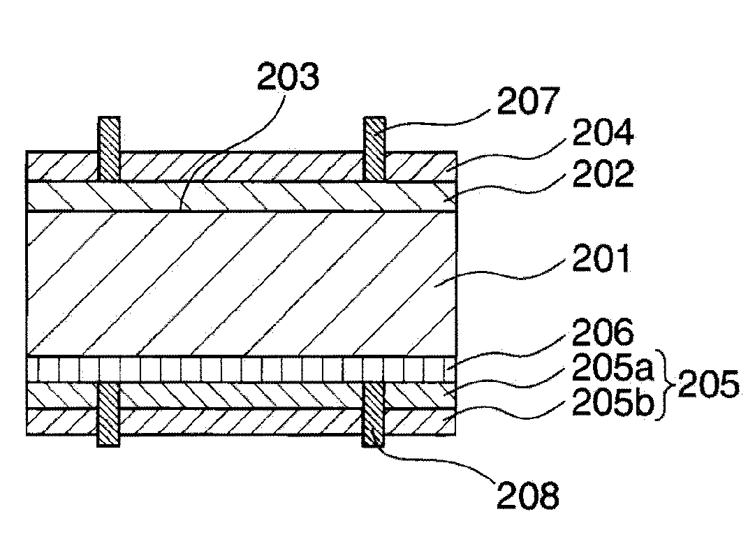
[0028]Now that an aluminum oxide film having a specific thickness is formed on a substrate surface, specifically the non-light-receiving surface of a p-type semiconductor substrate or the light-receiving surface of a n-type semiconductor substrate, a satisfactory passivation function and tight electrical contact between the substrate and the electrode are obtainable merely by the step of firing a conductive paste, which is a prior art technique. The invention omits the anneal step which is necessary in the prior art for the aluminum oxide film to exert a passivation effect, and is very effective for cost reduction.

Problems solved by technology

However, at the surface corresponding to the terminus of an atom array, an unstable energy level, also referred to as unsatisfied valence or dangling bond, develops because an adjoining atom to be bonded is not available.
The dangling bond is electrically active enough to capture an electric charge photo-created within silicon whereby the charge is extinguished, thus detracting from the performance of solar cells.
However, it is known that if a silicon nitride or analogous film having positive charges is applied to the surface of p-type silicon substrate, solar cell performance is degraded.

Method used


Image

  • Solar cell, method for manufacturing solar cell, and solar cell module
  • Solar cell, method for manufacturing solar cell, and solar cell module
  • Solar cell, method for manufacturing solar cell, and solar cell module

Examples


example

[0056]Experiments, Examples and Comparative Examples are given below for further illustrating the invention although the invention is not limited to the Examples.

experiment 1

Investigation of Electrode Contact Resistance

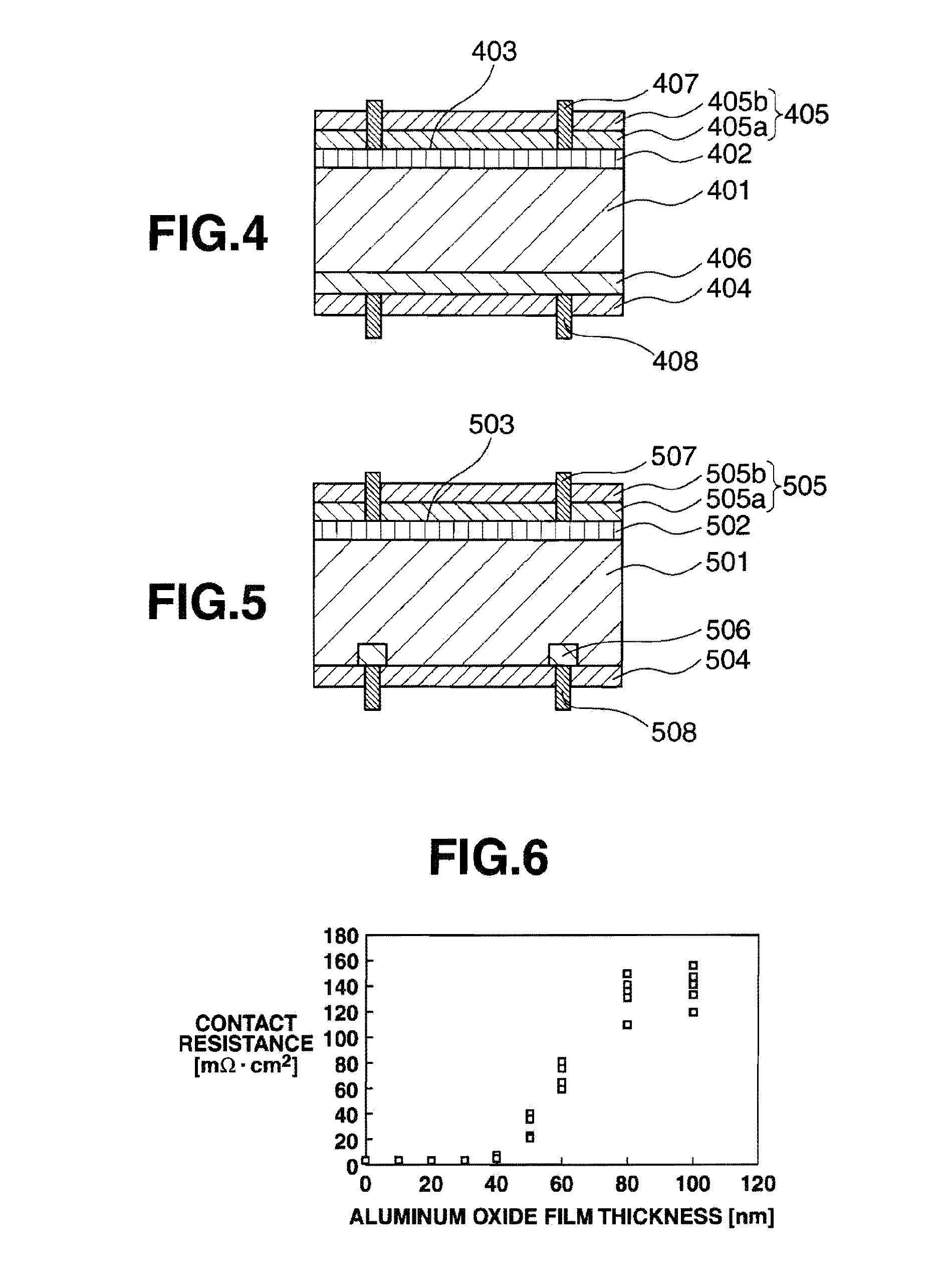
[0057]To investigate the thickness of an aluminum oxide film, first a conductive paste commonly used for the fire-through capability to silicon oxide film was used to examine its fire-through capability to aluminum oxide film. The fire-through capability can be evaluated in terms of contact resistance between the electrode and the silicon substrate.

[0058]Vapor phase diffusion of boron bromide was carried out on a textured p-type silicon wafer of 15 cm squares having a thickness of 240 μm, thereby diffusing boron therein to form a p+ layer. An aluminum oxide film was formed on the p+ layer by the ALD method, and a silicon oxide film was formed thereon by the plasma CVD method. The thickness of the silicon oxide film was adjusted such that the total thickness of aluminum oxide film and silicon oxide film was 100 nm. On these passivation films, a commercially available fire-through capability silver paste was printed in a comb-shaped pattern...

experiment 2

Investigation of Passivation Effect Upon Electrode Firing

[0061]Next, a test of measuring carrier life was carried out to examine the passivation effect versus thickness of aluminum oxide film.

[0062]On opposite surfaces of a p-type silicon wafer of 15 cm square having a thickness of 200 μm which had been mirror finished by acid etching, aluminum oxide films of varying thickness were formed by the ALD method. To impart the thermal hysteresis of electrode firing heat treatment, each sample was heat treated in a RTP furnace at a peak temperature of 800° C. for 3 seconds.

[0063]FIG. 7 diagrammatically illustrates the measurement results of effective carrier life before and after heat treatment. The effective carrier life is an overall carrier life including a carrier life in crystal bulk silicon and a carrier life at the silicon-aluminum oxide film interface, expressed in microsecond unit. In FIG. 7, the broken line with black squares designates the effective carrier life before heat trea...


PUM


Abstract

Disclosed is a solar cell which is provided with: a semiconductor substrate having a light-receiving surface and a non-light-receiving surface; a PN junction section formed on the semiconductor substrate; a passivation layer formed on the light-receiving surface and / or the non-light-receiving surface; and power extraction electrodes formed on the light-receiving surface and the non-light-receiving surface. The solar cell is characterized in that the passivation layer includes an aluminum oxide film having a thickness off 40 nm or less. As a result of forming a aluminum oxide film having a predetermined thickness on the surface of the substrate, it is possible to achieve excellent passivation performance and excellent electrical contact between silicon and the electrode by merely firing the conductive paste, which is conventional technology. Furthermore, an annealing step, which has been necessary to achieve the passivation effects of the aluminum oxide film in the past, can be eliminated, thus dramatically reducing costs.

Description

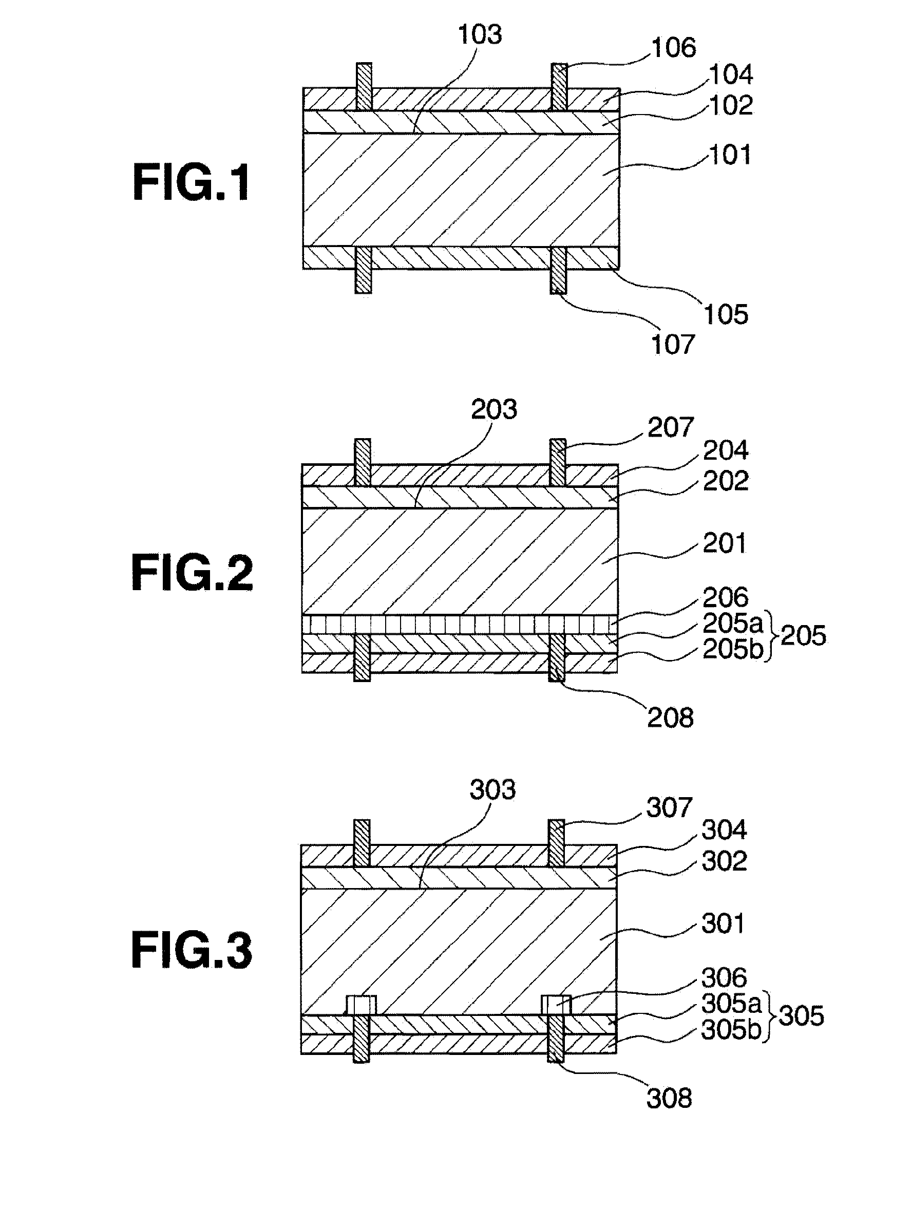
TECHNICAL FIELD[0001]This invention relates to a solar cell featuring high productivity, low cost, and high efficiency, a method for manufacturing the solar cell, and a solar cell module.BACKGROUND ART[0002]FIG. 1 schematically illustrates a p-type substrate solar cell as one example of prior art solar cells which are generally manufactured on a mass-scale using single crystal and polycrystalline silicon substrates. A pn junction 103 is formed by diffusing Group V element such as phosphorus into the light-receiving surface of a semiconductor substrate (silicon substrate) 101 in a high concentration to form a n-type layer 102. Dielectric films 104 and 105 having a lower refractive index than silicon are formed on both the major surfaces (light-receiving and non-light-receiving surfaces) of p or n-type silicon substrate, respectively, for more efficient containment of light. In these dielectric films 104 and 105, titanium oxide, silicon nitride, silicon carbide, silicon oxide, tin oxi...

Claims


Application Information

Patent Timeline
Patent Type & Authority Applications(United States)
IPC IPC(8): H01L31/042H01L31/18H01L31/0224H01L31/068
CPCH01L31/02167Y02E10/547H01L31/1868H01L31/068H01L31/022425Y02P70/50
Inventor HASHIGAMI, HIROSHIWATABE, TAKENORIOTSUKA, HIROYUKI
Owner SHIN ETSU CHEM IND CO LTD
Learn More