Antenna and wireless IC device

Active Publication Date: 2012-07-05
MURATA MFG CO LTD
View PDF4 Cites 22 Cited by
  • Summary
  • Abstract
  • Description
  • Claims
  • Application Information

AI Technical Summary

Benefits of technology

[0007]Therefore, preferred embodiments of the present invention to provide an antenna causing impedance matching with a wireless IC to be easily achieved and preventing the deterioration of a gain and the wireless IC device including the antenna.
[0022]According to various preferred embodiments of the present invention, since the auxiliary electrode is electrically connected to the loop electrode and located at a position along the loop electrode, the real portion of an impedance is large compared with a loop antenna based on a simple loop electrode. Therefore, it is easy to achieve impedance matching with the wireless IC, and it is possible to improve an antenna gain.
[0024]For example, the auxiliary electrode is disposed so as to follow the loop-shaped electrode from the vicinity of one feeding point of the loop electrode, and hence parallel resonance occurs due to a capacitance occurring between the loop electrode and the auxiliary electrode and the individual inductances thereof. In addition, because of this parallel resonance, it is possible to enlarge the real portion of an impedance in the vicinity of a resonance frequency. Therefore, it is easy to achieve matching with the wireless IC, and the antenna gain is improved.
[0025]Since, in the vicinity of the resonance (the above-mentioned parallel resonance) frequency of a circuit based on the loop electrode and the auxiliary electrode, currents flowing in the loop electrode and the auxiliary electrode are opposite to each other in phase, the antenna gain is deteriorated. Therefore, by deviating the above-mentioned resonance frequency from a frequency used in communication, it is possible to reduce the influence of the antenna gain deterioration.
[0026]An electrode is arranged so that the auxiliary electrode follows the outer side of the loop electrode, and hence it is possible to enlarge capacitance between electrodes, and it is possible to reduce an influence on an antenna directivity.

Problems solved by technology

However, since, in general, the loop antenna has an impedance whose real portion is small, there has been a problem that it is hard to achieve impedance matching with a wireless IC and a gain is easily deteriorated.
The above-mentioned problem is especially noticeable in a UHF frequency band, and the problem grows bigger in a wireless tag utilizing a UHF band.

Method used


Image

  • Antenna and wireless IC device
  • Antenna and wireless IC device
  • Antenna and wireless IC device

Examples


first preferred embodiment

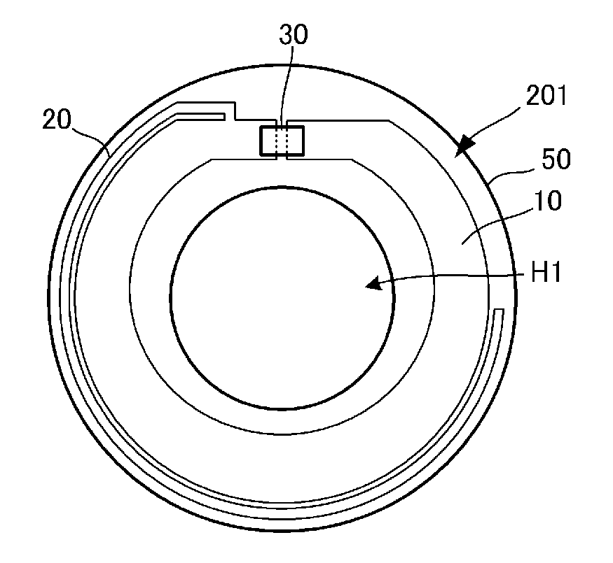
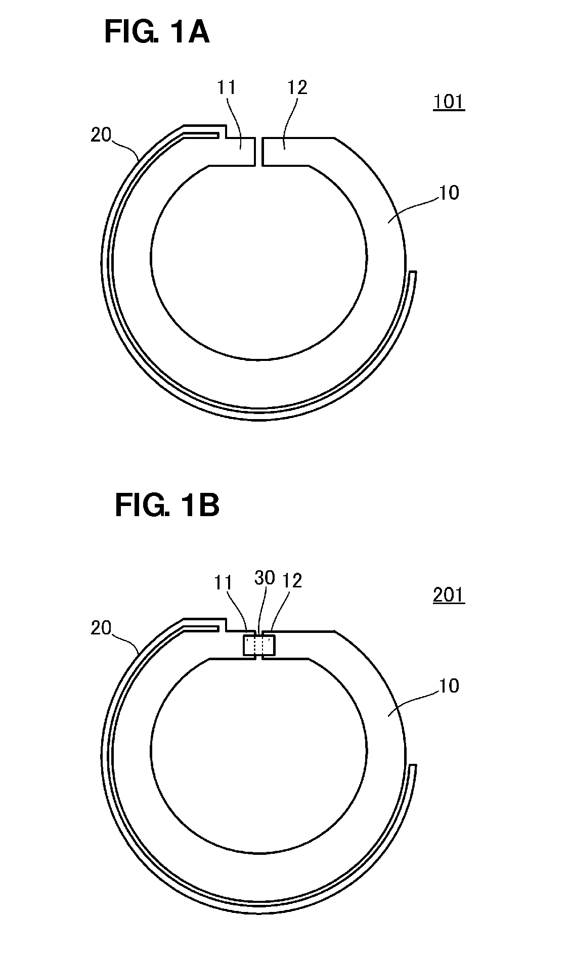
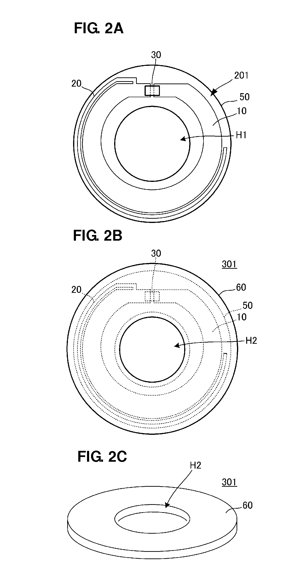
[0048]FIG. 1A is a plan view of an antenna 101 according to a first preferred embodiment, and FIG. 1B is a plan view of a wireless IC device 201 including the antenna 101.

[0049]The antenna 101 includes two feeding points 11 and 12, and includes a loop electrode 10 whose starting point and ending point are the feeding points 11 and 12, respectively, and that is arranged in a loop shape, and an auxiliary electrode 20 electrically connected to the loop electrode 10 and located at a position along the outer circumference of the loop electrode 10. The loop electrode 10 defines as a main radiation element.

[0050]The loop electrode 10 and the auxiliary electrode 20 preferably are copper foils patterned on a substrate, for example. The vicinities of both end portions of the loop electrode 10 are regarded as the feeding points 11 and 12. The first end portion of the auxiliary electrode 20 is electrically connected to the vicinity of one feeding point 11 of the loop electrode 10, and the auxil...

second preferred embodiment

[0079]FIG. 6 is the perspective view of a wireless IC 31 according to a second preferred embodiment of the present invention.

[0080]The example illustrated in FIGS. 1A and 1B is illustrated based on the assumption that the wireless IC 30 is a single semiconductor IC chip, for example. In the example in FIG. 6, the wireless IC 31 preferably includes a feed circuit substrate 40 and a wireless IC chip 30T. FIGS. 7-1A through 7-1H are diagrams illustrating the electrode pattern of each layer in the feed circuit substrate 40. FIG. 7-2 is an equivalent circuit diagram based on the feed circuit substrate 40 and a feed circuit.

[0081]The wireless IC chip 30T is mounted on the top surface of the feed circuit substrate 40. In such a state, the terminal electrodes of the wireless IC chip 30T are connected to terminal electrodes 43a, 43b, 44a, and 44b formed on the top surface of the feed circuit substrate 40.

[0082]FIGS. 7-1A through 7-1H are diagrams illustrating the electrode patterns of indivi...

third preferred embodiment

[0098]FIG. 8 is the plan view of an antenna 102 according to a third preferred embodiment of the present invention.

[0099]The antenna 102 illustrated in FIG. 8 includes the two feeding points 11 and 12, and includes the loop electrode 10 arranged in a loop shape and the auxiliary electrode 20 electrically connected to the loop electrode 10 and located at a position along the outer circumference of the loop electrode 10. The auxiliary electrode 20 is arranged along the outer circumference of the loop electrode 10 so as to circle the loop electrode 10 one time or more. In this way, the auxiliary electrode 20 may extend so as to circle the loop electrode 10 one time or more.

[0100]FIG. 9A is a diagram illustrating the distribution of the current intensity of the antenna 102 according to the third preferred embodiment. In this example, the directions of currents in individual portions are indicated by the directions of arrowheads, and current intensities are also indicated by the densitie...


PUM


Abstract

An antenna includes two feeding points, and includes a loop-shaped loop electrode and an auxiliary electrode electrically connected to the loop electrode and located at a position along the outer circumference of the loop electrode. The first end portion of the auxiliary electrode is electrically connected to the vicinity of one feeding point of the loop electrode. The second end portion of the auxiliary electrode is open. A resonant circuit is defined by the auxiliary electrode and the loop electrode to enhance the impedance of the antenna, compared with a case in which the antenna is configured using the simple loop electrode, and it is easy to achieve impedance matching with the wireless IC.

Description

BACKGROUND OF THE INVENTION[0001]1. Field of the Invention[0002]The present invention relates to an antenna and a wireless IC device. Specifically, the present invention relates to a loop-shaped antenna and a wireless IC device equipped therewith.[0003]2. Description of the Related Art[0004]As the structure of an antenna provided in a wireless tag, a loop antenna is known. In general, the loop antenna is configured using an electrode (conductor) formed in a loop shape beginning at a feeding point. A loop antenna is disclosed in “Antenna Engineering Handbook”, written and edited by The Institute of Electronics and Communication Engineers, published by Ohmsha, Ltd., Mar. 5, 1999, P. 20 to P. 22.[0005]However, since, in general, the loop antenna has an impedance whose real portion is small, there has been a problem that it is hard to achieve impedance matching with a wireless IC and a gain is easily deteriorated. Namely, while the real portion of the impedance of the wireless IC is wit...

Claims


Application Information

Patent Timeline
IPC IPC(8): H01Q11/12
CPCH01Q1/38H01Q5/371H01Q7/00
Inventor NOMURA, MASATOKATO, NOBORUDOKAI, YUYA
Owner MURATA MFG CO LTD
Why Eureka
Try Eureka