Microfabrication of high temperature microreactors
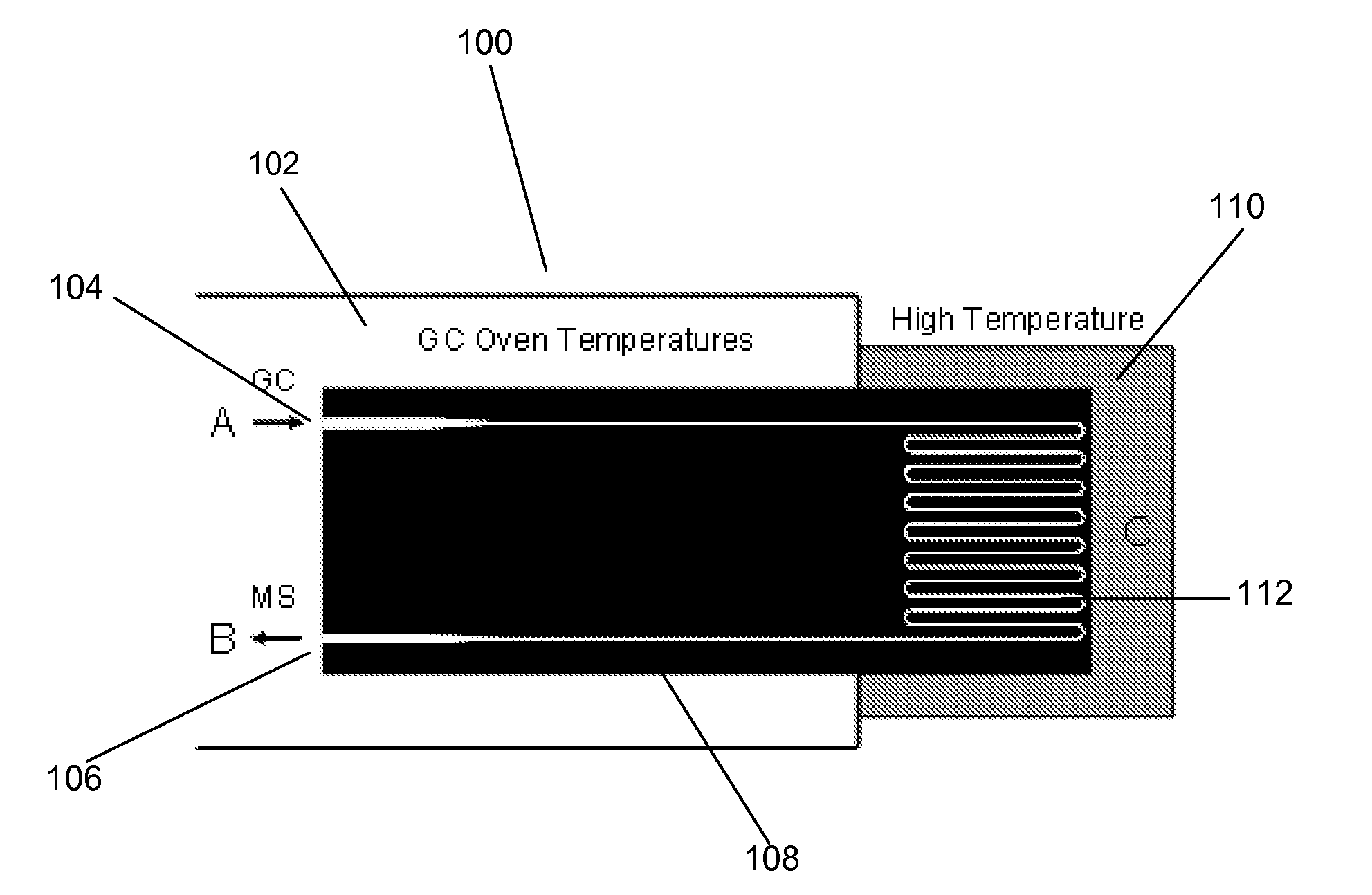
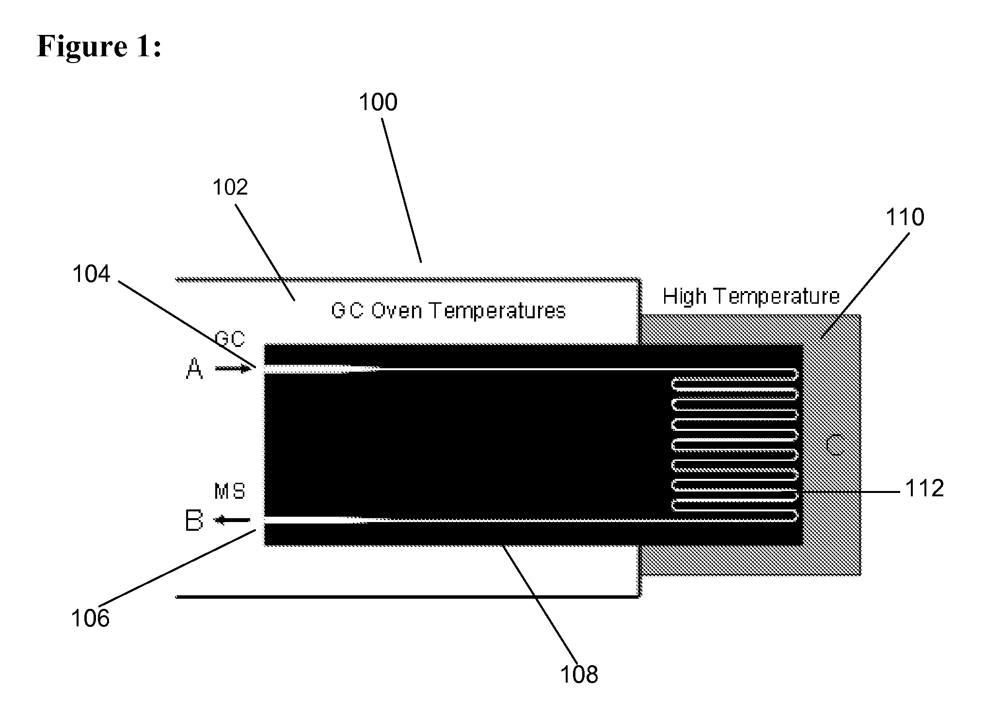
a micro-reactor and high-temperature technology, applied in the field of micro-fabrication of high-temperature micro-reactors, can solve the problems of inability inability to use tubes or capillary reactor designs, and the low end of the i.d. of the tube and capillary reactor is currently limited by the ability to physically fill the reactor, etc., to achieve stable isotopic composition analysis, robust operation, and more robust
- Summary
- Abstract
- Description
- Claims
- Application Information
AI Technical Summary
Benefits of technology
Problems solved by technology
Method used
Image
Examples
example 1
Photomask Generation
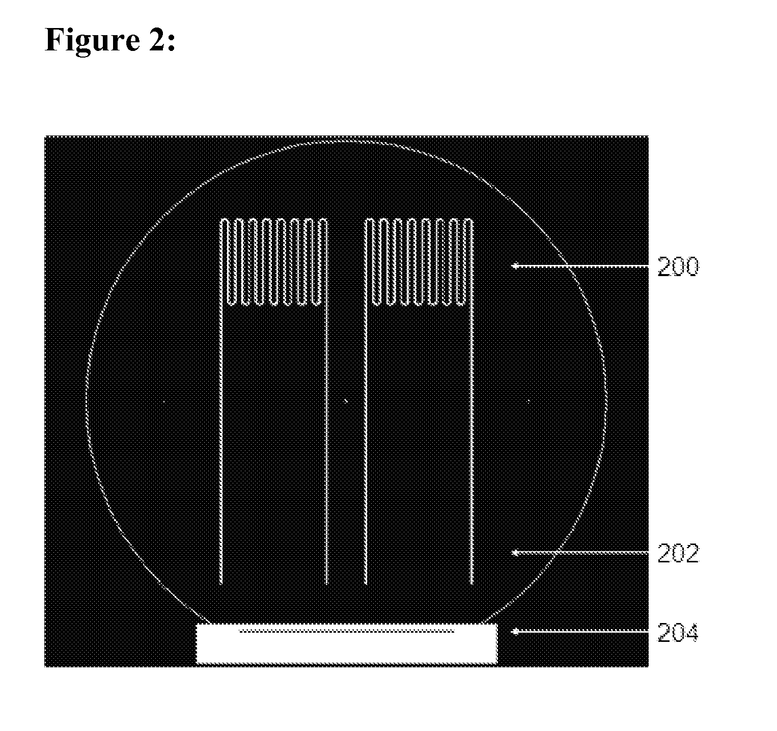
[0073]The CAD software utility Layout Editor™ (freeware) was used to create a drawing and an exported graphic data system (GDSII) file of the microreactor passage design. The file was used to guide the exposure of photoresist on a chromium coated, 5 inch (124 mm) square glass substrate using a GCA Mann 3600 Pattern Generator (D. W. Mann / GCA Corporation, USA). The photoresist was developed using 300 MIF developer (Hoechst Celanese, Somerville N.J.) for 120 sec, water rinsed and spin dried. The exposed chrome layer was removed using CR-14 Chromium Etchant (Cyantek Corporation, Fremont Calif.) for 120 sec, water rinsed, and spin dried. Photoresist was subsequently removed by hot stripping in a 75° C. bath containing propylene glycol, n-methyl-pyrrolidone (NMP), and tetramethyl ammonium hydroxide (TMAH) for 20 min, water rinsed, and spin dried.
example 2
Furnace Processing
[0074]Double side polished 100 mm diameter, 1.0 mm thick, synthetic amorphous high purity fused silica wafers (Corning 7980, Mark Optics, Santa Ana Calif.) were thoroughly cleaned, as used for metal oxide semiconductor technology, before furnace processing by sequential immersion in a base (6 L H2O, 1 L NH4OH, 1 L H2O2), acid (6 L H2O, 1 L HCl, 1 L H2O2), and HF (20:1 H2O:HF) bath for 10 min, 10 min, and 15 sec, respectively. The wafers were water rinsed to 16 MΩ after each bath then spun dry. Low pressure chemical vapor deposition (LPCVD) was used to deposit a layer of approximately 250 nm of amorphous Si using a furnace processing tube (Cryco, Austin Tex.). Three different Si deposition recipes (SR) were tested. SR1 included a 150 sccm flow of silane (SiH4) at 140 mTorr and 560° C. for 100 min. SR2 included a 150 sccm flow of SiH4 at 140 mTorr and 540° C. for 250 min. And SR3 included a 150 sccm flow of SiH4 and a 10 sccm flow of 1.5% PH3 / N2 (PH3:SiH4 ratio of 1×...
example 3
[0075]The LPCVD Si surface of each high purity fused silica wafer was dehydrated at 115° C. for 1 min on a hot-plate and then cooled. Wafers were then treated and manually spin coated with a solution containing 20% hexamethyldisilazane and 80% propylene glycol monomethyl-ether acetate (MicroPrime P-20 Primer, Shin-Etsi Chemical Company, Japan) as an adhesion promoter, and then spin coated with a 1.3 μm layer of broadband photoresist (Shipley Microdeposit S1813, Rohm & Haas, Philadelphia Pa.) at a rotational speed of 4000 rpm for 60 sec. Each wafer was then immediately soft-baked at 115° C. for 1 min on a hot-plate and then cooled. The photoresist on the wafers was exposed using 405 nm light (20 mW / cm2) for 3.0 sec by means of “soft” contact with the photomask using a HTG System III-HR Contact Aligner (Hybrid Technology Group Inc., Scotts Valley Calif.) The photoresist was developed using 300 MIF developer for 120 sec, water rinsed and spin dried. The exposed am...
PUM
| Property | Measurement | Unit |
|---|---|---|
| inner diameters | aaaaa | aaaaa |
| inner diameters | aaaaa | aaaaa |
| lengths | aaaaa | aaaaa |
Abstract
Description
Claims
Application Information
 - R&D
- Intellectual Property
- Life Sciences
- Materials
- Tech Scout
- Unparalleled Data Quality
- Higher Quality Content
- 60% Fewer Hallucinations
Browse by: Latest US Patents, China's latest patents, Technical Efficacy Thesaurus, Application Domain, Technology Topic, Popular Technical Reports.
© 2025 PatSnap. All rights reserved.Legal|Privacy policy|Modern Slavery Act Transparency Statement|Sitemap|About US| Contact US: help@patsnap.com


