Thin-film transistor forming substrate, semiconductor device, and electric apparatus
a technology forming substrates, which is applied in the direction of transistors, electrical equipment, semiconductor devices, etc., can solve the problems of parasitic capacitance (electrostatic capacitance) formed between multi-layer wirings of tft elements, power consumption increases, and weight, etc., and achieves and high precision of thin film transistors
- Summary
- Abstract
- Description
- Claims
- Application Information
AI Technical Summary
Benefits of technology
Problems solved by technology
Method used
Image

Examples
first embodiment
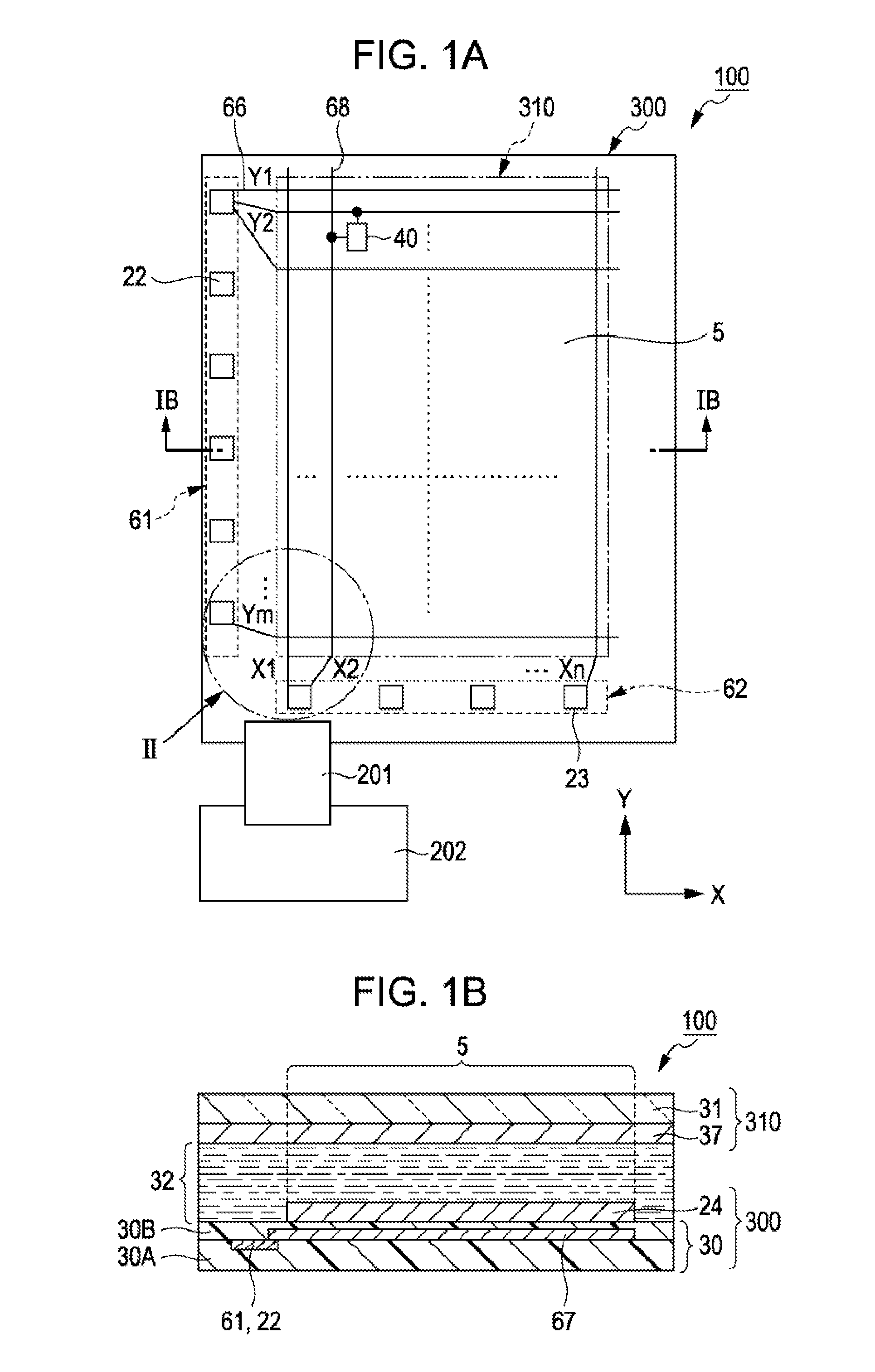
[0076]FIG. 1A is a plan view showing a schematic configuration of a component substrate, which configures an electric apparatus, according to a first embodiment, and FIG. 1B is a cross-sectional view showing a schematic configuration of the electric apparatus.
[0077]As shown in FIGS. 1A and 1B, in an electro-optical device (electric apparatus) 100, an electro-optical element (functional element) 32 is interposed between a component substrate 300 and an opposing substrate 310 that respectively have flexibility.
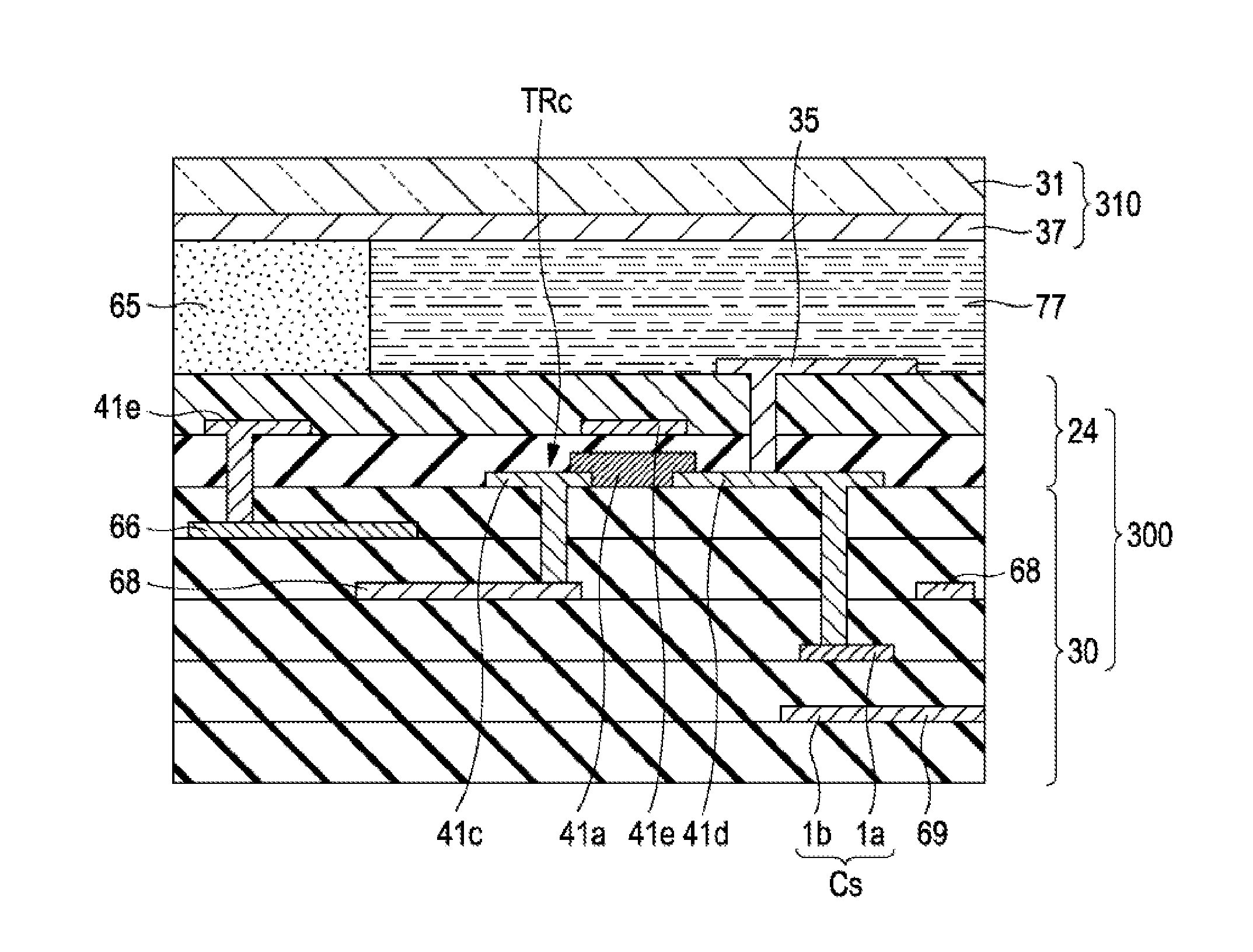
[0078]The component substrate (semiconductor device) 300 is configured by a first substrate (thin-film transistor forming substrate) 30 that is formed from a plurality of laminated base members and a driving circuit layer 24. The first substrate 30 is configured so as to include a wiring layer 67 that has scanning lines, data lines, holding capacitors, and the like, a scanning line driving circuit 61, and a data line driving circuit 62. In addition, on the uppermost layer, at le...
second embodiment
[0154]Next, the configuration of a component substrate according to a second embodiment will be described.
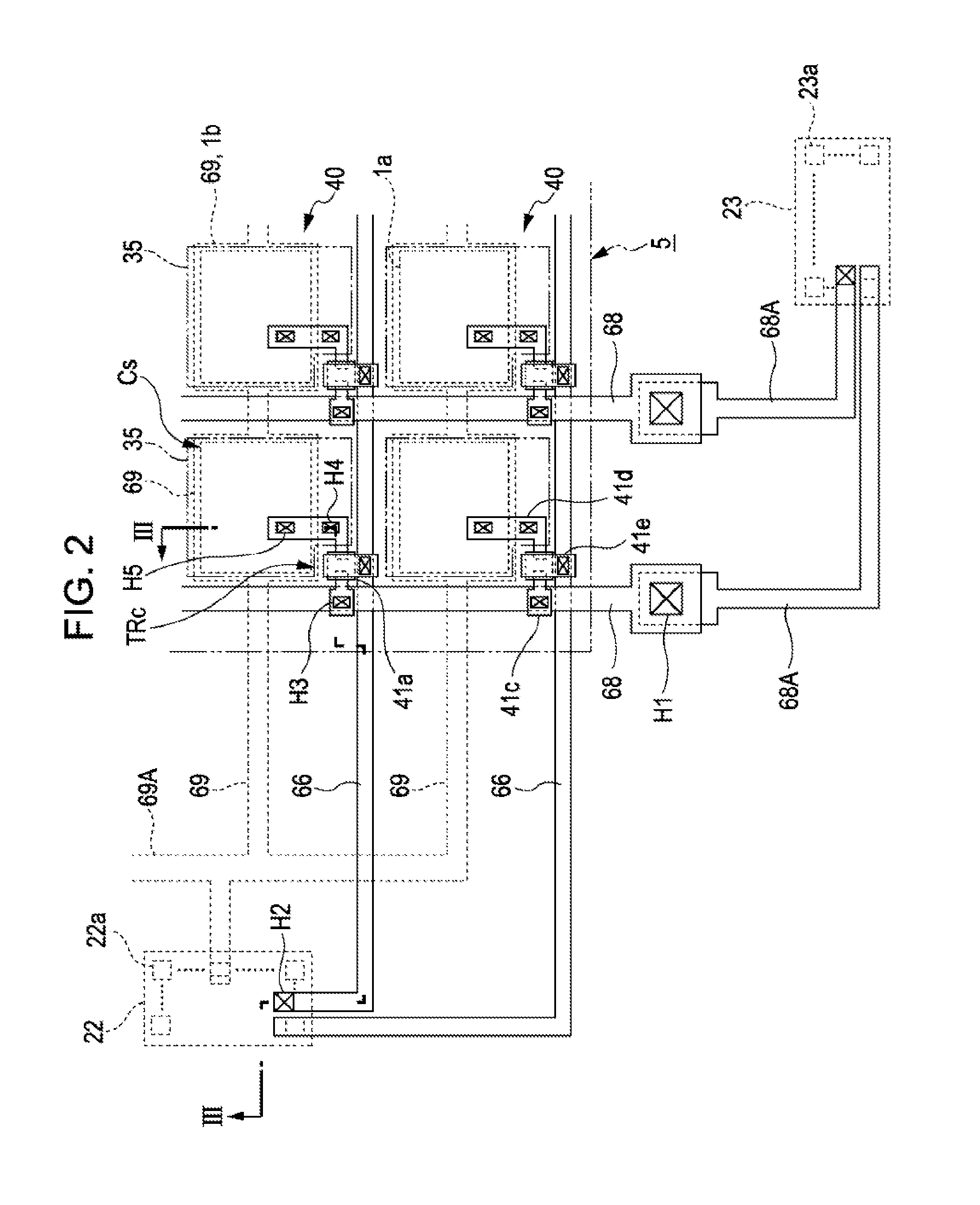
[0155]FIG. 8 is a plan view showing a pixel configuration formed on a component substrate according to the second embodiment. FIG. 9 is a cross-sectional view taken along line IX-IX shown in FIG. 8. A pixel TFT has a bottom-gate and bottom-contact structure. Holding capacitor connection portions 69a and 69b are disposed on a first substrate 30 in the same layer as that of a gate electrode 41e.
[0156]As shown in FIGS. 8 and 9, in this embodiment, inside the first substrate 30 configuring a component substrate 301, holding capacitors Cs1 and Cs2 are buried over two pixels 40A and 40B adjacent to each other. Each one of the holding capacitors Cs1 and Cs2 is configured by one of one pair of the holding capacitor electrodes 2a that are formed in different layers and a holding capacitor electrode 2b arranged therebetween. Each of the holding capacitor electrodes 2a and 2b represents a...
third embodiment
[0166]Next, the configuration of a component substrate according to a third embodiment will be described.
[0167]FIG. 10 is a plan view showing a pixel configuration of the component substrate according to the third embodiment. FIG. 11 is a cross-sectional view taken along line XI-XI shown in FIG. 10.
[0168]As shown in FIGS. 10 and 11, in this embodiment, a gate insulating film 41b of a control transistor TRc and a protection layer 42 are not formed on the entire surface of the component substrate 302 (first substrate 30) but are disposed for each pixel.
[0169]In a part (near an intersection of the scanning line 66 and the data line 68) of the pixel area, the gate insulating film 41b is selectively formed so as to cover the entire semiconductor layer 41a formed on the first substrate 30 and parts of the source electrode 41c and the drain electrode 41d. A gate electrode 41e is disposed at a position located on the gate insulating film 41b that faces the semiconductor layer 41a.
[0170]In ...
PUM
 Abstract
Description
Claims
Application Information
 - Generate Ideas
- Intellectual Property
- Life Sciences
- Materials
- Tech Scout
- Unparalleled Data Quality
- Higher Quality Content
- 60% Fewer Hallucinations
Browse by: Latest US Patents, China's latest patents, Technical Efficacy Thesaurus, Application Domain, Technology Topic, Popular Technical Reports.
© 2025 PatSnap. All rights reserved.Legal|Privacy policy|Modern Slavery Act Transparency Statement|Sitemap|About US| Contact US: help@patsnap.com